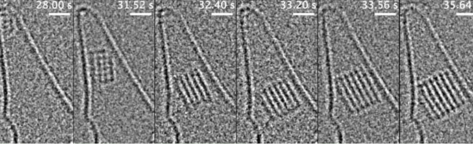
Capture dynamic processes during in-situ TEM experiments with the Gatan OneView IS camera, at up to 25 fps with 16 MP images. In this example, researchers at the University of Tokyo observed crystal nucleation and growth at atomic scale.
Register now for MMC 2021 (online) microscopy conference. Visit our virtual booth at the exhibition!
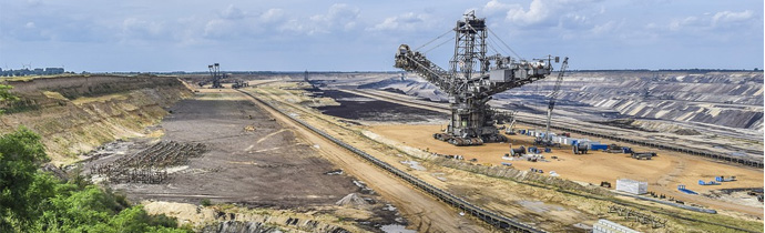
Precise, accurate trace analysis of geological materials including rocks, minerals & soils with the Bruker S8 TIGER Series 2 WD_XRF & GEO-QUANT Traces, a dedicated solution package.

Combined SEM-EDS can be used to locate and identify contamination quickly and easily. The Thermo Scientific Axia ChemiSEM fully integrates the two techniques.

As the steel industry works to reduce its carbon footprint, working towards climate neutral production, elemental analysis is required to maintain and monitor product quality. OES (Optical Emission Spectrometry) is a useful metals anlaysis technique to monitor concentrations of vital elements at all stages of production and recycling, as processors work to reduce emissions without compromising quality or steel grades.
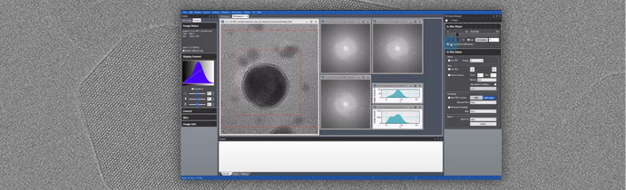
A series of video tutorials demonstrating how to use Gatan’s IS player, part of GMS 3 (Gatan Microscopy Suite) software for TEM/SEM.
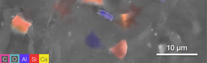
SEM-EDS can be used to characterise the composition of polymer composites. This is useful in failure analysis, to detect and identify contaminants and defects, and to check homogeneity.
Map defect distribution and variations for process development of materials for electronic / optoelectronic devices. CL is ideal for materials not suitable for photoluminescence spectroscopy.

The EIGER2 R 250K is an HPC (Hybrid Photon Counting) pixel detector for the Bruker D8 ADVANCE and DISCOVER XRD systems.
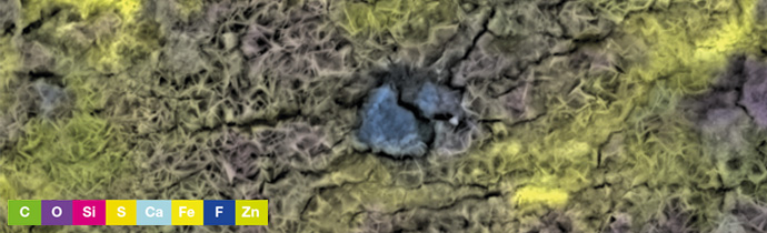
How SEM/EDS is used in failure analysis of steel, with examples of bend test failures, coating defects and corrosion in the automotive industry.