Only 30 seconds from sample loading to imaging.
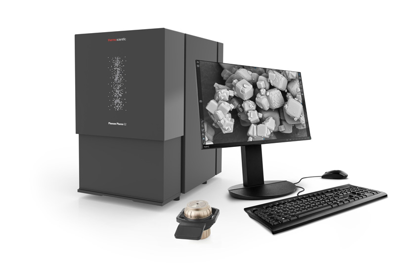
The Thermo Scientific Phenom Pharos is a desktop SEM (Scanning Elecron Microscope) with an Field Emission (FEG) source for crisp, high-brightness images. It’s much easier to use and install than a typical FEG-SEM, making the benefits of an FEG source accessible to everyone.
Only 30 seconds from sample loading to imaging.
Robust and compact.
With low energy imaging for soft, sensitive and insulating materials.
2.0 nm images.
Optional EDS
The Phenom Pharos Desktop SEM is designed to make FEG-SEM accessible to everyone, delivering crisp, high-brightness images.
The installation process is straightforward, requiring just a solid table and a regular power supply. The UPS (Uninterrupted Power Supply) is integrated, protecting the system from any power failures. Initialisation starts automatically when the power’s switched on.
After loading a sample, an optical image is available immediately for navgation. When you switch to SEM mode, an image appears in 30 seconds. The new interface on the G2 model displays a full-screen, highly detailed 24″ image.
Training takes less than an hour. Master students, visitors or researchers not trained on high-end FEG SEMs can easily acquire high quality images with the Phenom Pharos.
With a voltage range down to 1 kV you can image soft, insulating and beam-sensitive samples, such as polymers. There’s no need to apply any special coatings or prepare the samples.
The Phenom Pharos G2 also offers a resolution of 2.0 nm at 20 kV. This reveals features that may be missed by other tabletop or tungsten SEMs, such the shape of nanoparticles or imperfections in coatings.
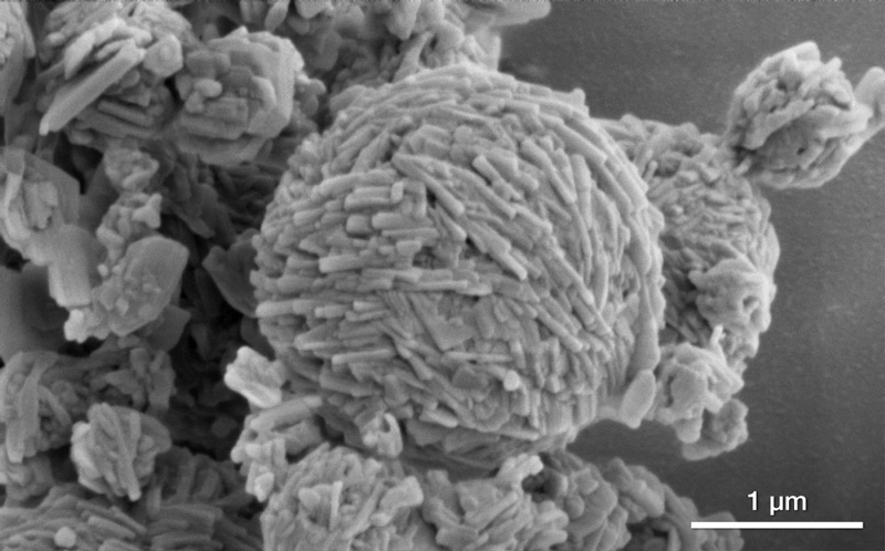
Silver Nanostructure
A recorded webinar from Thermo Scientific about how to match the features and specification of a SEM to the requirements of your application.