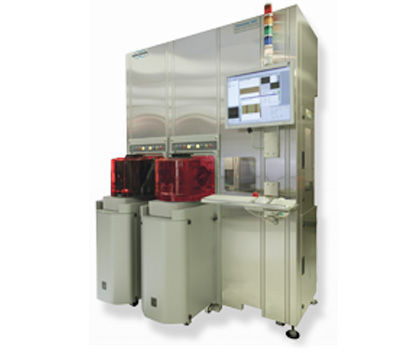
 Bruker Dimension AFP
World’s Only Fab-Based AFM Metrology System
The Bruker Dimension AFP is the world’s only fab-based metrology tool for CMP profiling and etch depth metrology, for current and advanced technology nodes.
Combining the high resolution of AFM with the long scan capability of atomic force profilers, the instruments monitors etch depth, dishing and erosion on sub-micron features with unmatched repeatability. An alternative to costly wafer cross-sectioning, the Dimension AFP delivers the highest possible performance for device characterisation.
- AFM resolution combined with the long-scan capability of an atomic force profiler
- Fastest throughput of any AFM or profiler
- Unsurpassed repeatability for in-line STI, W, Cu and CMP metrology
- Replaces costly, destructive cross-sectioning techniques
- Etch measurements in minutes
- Non-destructive measurement of high-aspect-ratio features
Contact us for more information and quotes:
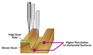
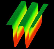
Deep Trench (DT) Mode measures deep semiconductor trench structures 90 nm and below. It is an adaptive scan method, collecting data only when specified conditions are met.
Applications
Chemical Mechanical Planarisation
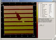
Chemical mechanical planarisation (CMP) is a process where an abrasive pad polishes a surface, using a physically and chemically active slurry. In semiconductor manufacture, the overall flatness of the surface must be controlled to ~1nm, regardless of any underlay contrast in material or geometry. Atomic Force Profilers (AFPs) can be used to determine both the localised dishing and overall layer erosion (D&E). The Bruker Dimension AFP can control the production process for CMP on all layers, including shallow trench isolation (STI), tungsten plug, contacts & vias or copper lines.
Depth Metrology
In many production processes, the depth or height of the output needs to be controlled. This is especially important in semiconductor etch processes, where nanometre variation can cause significant problems eg short/open circuit, high leakage current and loss of contact. With atomic z-resolution, AFM is ideal for process data in advanced semiconductor manufacturing.
Roughness
Deposition processes such as High-K metal gate for semiconductor transistor fabrication, or low-k porous dielectric materials, and the introduction of new materials, requires information about the quality of the films and materials being deposited. Surface roughness characterisation provides insights for R&D, as well as for quality control in production.
Bruker automated AFMs can be used to collect roughness data in-line on 150mm, 200mm, 300mm and up to 450mm wafers. This same technique can also be used by semiconductor and ELD manufacturers to check incoming substrate quality.
Defect Review
Traditional inspection systems identify only the location of a defect. It is then necessary to use a review technique to determine other characteristics such as size, shape and composition. Bruker automated AFMs can automatically collect AFM images at known defect locations, producing a 3D profile of the defect. This is useful for defect repair and locating cause of defect. Recipes can be created directly from defect files for convenience and increased productivity.