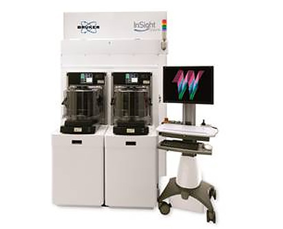
 Bruker InSight 3D AFM
Metrology for Process Control – 45nm and Below
The Bruker InSight 3D AFM measures CD, depth and CMP metrology in semiconductor production. Perform non-destructive, high-resolution 3D measurements of critical semiconductor features with unparalleled accuracy and precision.
The system takes a new approach, with unique in-line 3D Metrology (LWR, LER) and the lowest measurement uncertainty for CD, Depth and Sidewall Angle on critical layers, such as Shallow Trench Isolation, Gate and FinFet structures. The InSight 3D AFM overcomes the limitations of CD-SEM and Optical CD technologies, with no bias variation issues affecting CD measurement.
Contact us for more information and quotes:
Applications
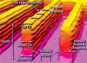
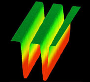
CD Metrology
Control of device critical dimension (CD) is required in the fabrication of devices including nano-electronics, MEMS and optoelectronics. CD control is directly related to device performance (transistor speed, MEMS efficiency, optoelectronic transmission, etc). The Bruker Insight 3D AFM provides TEM-level sidewall information for CD process control and SEM-level information for line width variability and edge roughness. There is no damage to the sample and no preparation is required, so tests can be performed before and after processes, eg resist & post-etch profile comparison.
Depth Metrology
In many production processes, the depth or height of the output needs to be controlled. This is especially important in semiconductor etch processes, where nanometre variation can cause significant problems eg short/open circuit, high leakage current and loss of contact. With atomic z-resolution, AFM is ideal for process data in advanced semiconductor manufacturing.
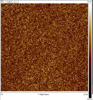
Roughness
Deposition processes such as High-K metal gate for semiconductor transistor fabrication, or low-k porous dielectric materials, and the introduction of new materials, requires information about the quality of the films and materials being deposited. Surface roughness characterisation provides insights for R&D, as well as for quality control in production.
Bruker automated AFMs can be used to collect roughness data in-line on 150mm, 200mm, 300mm and up to 450mm wafers. This same technique can also be used by semiconductor and ELD manufacturers to check incoming substrate quality.
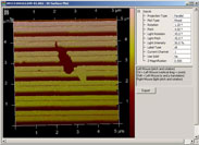
Defect Review
Traditional inspection systems identify only the location of a defect. It is then necessary to use a review technique to determine other characteristics such as size, shape and composition. Bruker automated AFMs can automatically collect AFM images at known defect locations, producing a 3D profile of the defect. This is useful for defect repair and locating cause of defect. Recipes can be created directly from defect files for convenience and increased productivity.