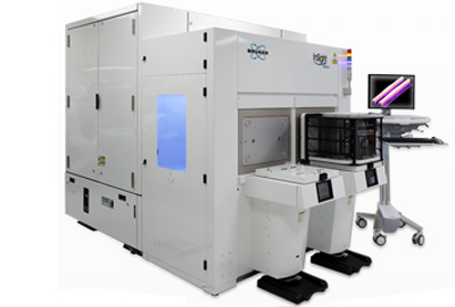
 Bruker InSight-450 3D AFM
AFM for Metrology of 450mm Wafers
Based on the established InSight 3D AFM platform for 300mm, the InSight-450 3D AFM is designed for 450mm wafers. Measure a broad range of roughness, depth and CD parameters, including:
- Bare wafer process validation
- Roughness characterisation and pit/bump/scratch defect metrology
- Incoming substrate qualification
- Thin film and epitaxial deposition performance with micro/nano roughness and angstrom-level step height precision
- Etch depth metrology for process development and control
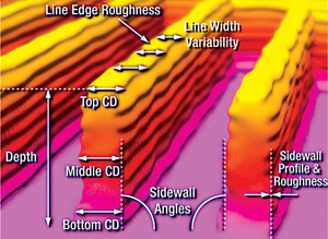
- In-line resist profile measurements of CD, SWA, and LER with full TEM-like profiles
- CMP flatness performance to monitor dishing and erosion.
Perform all of these measurements using a single instrument, thereby reducing your overall costs for metrology. No modelling is required, there is no material or wafer damage and the system is fully NIST traceable. The InSight-450mm AFM is ideal for 450mm process development, with scalability to 450mm wafer production.
Contact us for more information and quotes:
InSight-450 3D AFM reference metrology
Superior Critical Dimension, Depth and Roughness Metrology
The Bruker InSight-450 3D AFM is the most advanced automated AFM platform for in fab and full wafer metrology. The system includes the benefits of Bruker’s InSight AFM platform, extended to 450mm wafers, including a high-precision X-Y air bearing stage, high speed DSP automated tip exchange and patented CD (critical dimension) AFM control. The InSight-450 meets or beats the performance of the 300mm system, with minimal effect of scaling on AFM performance.
- Reference metrology for crucial CD elements including gate, shallow trench isolation (STI) union dual-damascene structures, sidewall angles, line-edge variation and more.
- Lowest measurement uncertainty for critical dimension and sidewall angle (SWA) metrology.
- Full wafer coverage, TEM-like accuracy and no wafer damage.
- Fully automated, including wafer registration, tip exchange, tip qualification and recipes.
- AFM resolution for bare wafer and thin film roughness characterisation.