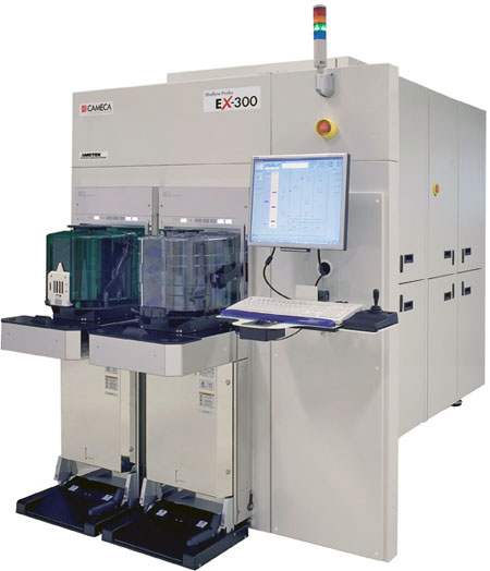
EX-300 Shallow Probe
LEXES-based semiconductor compositional metrology system
The CAMECA EX-300 Shallow Probe is a front-end semiconductor compositional metrology system for 22nm node and beyond. It’s installed at top-ten semiconductor fabrication facilities worldwide.
The EX-300 uses LEXES (Low energy Electron induced X-ray Emission Spectrometry) technology to measure chemical composition at the surface and near surface. A single system controls both composition and thickness, all kinds of stacks (mono or bi-layer, with/without capping) as well as production and blanket wafers.
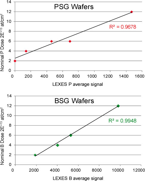
- Ultra shallow implants – Monitor low energy, high concentration implants.
- Strained silicon process control – Measure chemical composition and thickness of epitaxial layers (eg B:SiGe and P:SiC) with no limits on layer composition.
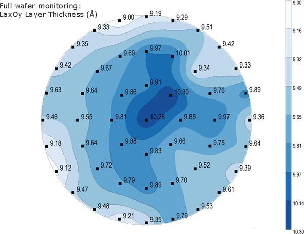
- HKMG metrology – Control both the oxides and metal with a single EX-300.
Contact us for more information and quotes:
+44 (0)1223 422 269 or info@blue-scientific.com
Features
- Robust, flexible pattern recognition
- Optimised light source & optics
- Zooming capabilities
- Small pad analysis (30×30μm)
- Non-contact
- Non-destructive
- High brightness LaB6 gun
- Dense, highly focussed probe
- Optimised MTTR (mean time to recovery)
- Ergonomic design for fast maintenance
- Ultimate long-term stability
- Optimised pumping system
- Define parameters to monitor automatically
Accelerate Time-to-Market
Bring logic and memory devices to market sooner:
- Control your front-end processes: HKMG, SiGe(B), SiC(P), implants.
- Select key process parameters during device development.
- Shorter ramping phase to enter mass production faster.
Save Money
Increase yield in high volume production:
- Catch process excursions with early measurement on wafer products.
- Save weeks of production output.
- Reduce product loss.