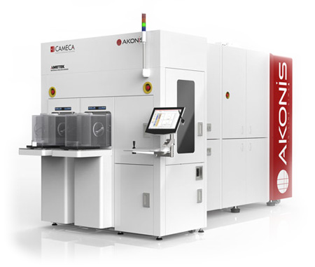
CAMECA AKONIS
Fully automated SIMS for metrology on semiconductor fabrication lines
The CAMECA AKONIS SIMS system for composition measurement fills a critical gap in semiconductor fabrication processes, working directly on the manufacturing line:
- High throughput
- High precision detection
- Implant profiles
- Composition analysis
- Interfacial data
AKONIS features a very high level of automation. This ensures repeatability across tools for fab level process control and tool-to-tool matching.
Contact us for more information and quotes:
+44 (0)1223 422 269 or info@blue-scientific.com
Contact Us <a href=”#” target=”_brochure” class=”button brochure product-form” rel=”noopener”>Brochure from CAMECA</a>
“We are proud to support key players in semiconductor technology and will continue to further improve our compositional metrology solutions so our customers can better control their next generation device development and manufacturing.
AKONIS is the culmination of more than 50 years of experience in ion instrumentation and over 30 years of close partnerships with leading semiconductor manufacturers.”
Dr. Jesse Olson, CAMECA
Features
- Fully automated set-up and acquisition routines.
- Fast, within-fab analysis without compromising sensitivity.
- EXtremely Low Impact Energy (EXLIE) ionic column technology (< 150 eV).
- Full wafer handling system.
- High resolution stage for measurements on pads down to 20 μm.
AKONIS complements the CAMECA IMS Wf/SC Ultra and SIMS 4550 quadrupole SIMS used in characterisation labs in the semiconductor industry.
Maximising yield on N5 and beyond
- High resolution composition and fast dopant depth profiling of SiGe and SiP multilayer stacks.
- Unrivalled in pad detection limits down to 20 μm.
- Reduces time to feedback data to the process line by >97%.
- Measures blanket and patterned full wafers.
- < 2 μm position accuracy, with a pattern recognition engine and high resolution interferometric stage.
- Build intuitive recipes with a unique material database
- SEMI certified (S2/S8, E4, E5, E39, E84, etc).
- Low cost of ownership.
Self-Focusing SIMS
Self-focusing SIMS was found to be ten times faster for characterising nanometre-size features than direct methods such as TEM and APT. More details…