A New Method for Characterising Nanometre-Sized Semiconductor Structures
Self-focusing SIMS is a new technique for measuring the composition of semiconductors and SiGE devices. It’s proven to be ten times faster than studying nanometre-scale features with direct measurement techniques.
Blue Scientific is the official distributor of CAMECA elemental and isotopic microanalysis instruments in the UK, Ireland and Finland. For more information or quotes, please get in touch.
More about SIMS
Contact us on +44 (0)1223 422 269 or info@blue-scientific.com
Characterising Semiconductor Transistors
Characterisation of semiconductor transistors can be challenging – with new devices their size is shrinking smaller and smaller. Metrology tools need a lateral resolution of just a few nanometers, as well as high depth resolution – together with high sensitivity.
Self-Focusing SIMS
Dynamic Secondary Ion Mass Spectrometry (SIMS) delivers high depth resolution at low primary impact energies (≤500 eV).
However, it uses a micron-sized beam to probe nanometre sized structures. A way of overcoming the beam size limitation is to localise the signal emitted by the device (laterally and by depth). This involves specifically tracking the molecular secondary ions emitted from the 3D area of interest. This new method is known as Self-Focusing SIMS.

Example: Characterising SiGe
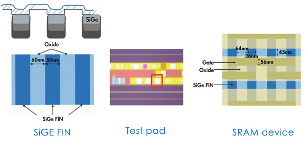
In this example, four test samples were produced by the same SiGe growth recipe. These were used to investigate a micro-loading growth effect and validate a new quantification model. The samples used were:
- SiGe blanket wafer.
- SIMS pad in the scribe line (50×60 μm2) which is larger than the beam size.
- Equally spaced, uniformly boron doped, vertical SiGe FIN structure with evenly spaced SiGe and Si3N4.
- SRAM device with SiGe structure occupying 11% of the total analysis area.
Self-Focusing SIMS was found to be around ten times faster than studying the small features directly with a method such as TEM or APT.
SIMS averages over many such structures, so the signal-to-noise is high. This means it does not provide information about compositional variation. However, the results are more statistically reliable than TEM and APT.
Application Note
More details about this experiment are available in an application note from CAMECA:
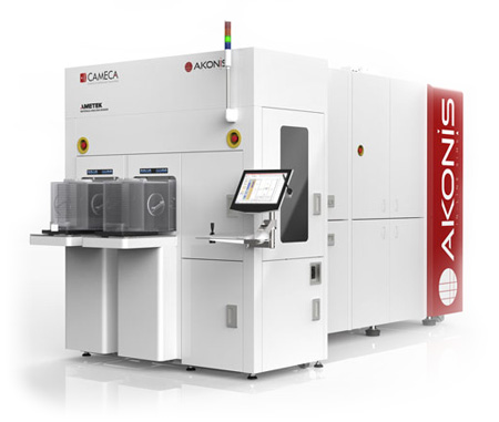
CAMECA AKONIS
- High throughput, high precision SIMS for implant profiles, composition analysis and interfacial data.
- Runs directly in the semiconductor manufacturing line.
- Fully automated set-up and acquisition routines.
- Fast, within-fab analysis without compromising sensitivity.
- Measurements on pads down to 20 μm.

The AKONIS complements the CAMECA IMS Wf/SC Ultra and the SIMS 4550 quadrupole SIMS, which are also used in semiconductor industry characterisation labs.
More Information
Blue Scientific is the official distributor of CAMECA SIMS systems in the UK, Ireland and Finland. We’re available to answer all your questions and provide quotes – just get in touch:


