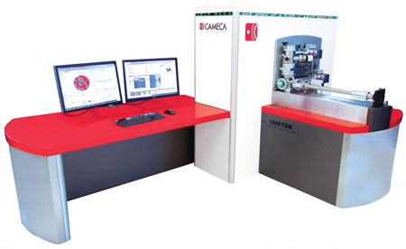
LEAP 5000
3D Atom Probe Microscope
The CAMECA LEAP 5000 is a 3D Atom Probe Microscope. LEAP (Local Electrode Atom Probe) microscopes analyse materials in 3D with near-atomic resolution. Gain insights into how a material’s nanostructure affects its functional properties. This helps relate phenomena on the nano-scale to properties at the macro-scale.
The LEAP 5000 collects nanoscale information from a microscale dataset in just a few hours. Measure a wide variety of metals, semiconductors and insulators, detecting >40% extra atoms per nm3.
- Unmatched sensitivity
- Large field-of-view and detection uniformity
- Multi-hit detection capabilities for accurate compositional measurement
- Ultra-high speed data acquisition with a fast, variable repetition rate
- Robust, ergonomic platform
- Real-time monitoring for high quality results
- Advanced laser control algorithms to maximise yield
What is Atom Probe Tomography?
Contact us for more information and quotes:
+44 (0)1223 422 269 or info@blue-scientific.com
Metals and Advance Materials Research
- Steels
- Nanowires
- Aluminum alloys
- Nickel-based alloys
- Zirconium-based alloys
- Superalloys
- Coatings
- Precipitates and clusters
- Grain and phase boundaries
- Precipitate-hardened materials
Analyse materials in 3D with atomic resolution. Data can be used to correlate properties (eg strength, heat transfer, irradiation damage, carrier lifetime) with nanostructural factors. The mass resolution is high enough to differentiate elements from their isotopes.
Compositional Analysis
With CAMECA’s cluster analysis algorithms you can calculate elemental concentrations within precipitates and clusters. These can be as small as 10 atoms across. You can define isoconcentration levels to limit analysis to specified boundaries.
Example: 3D Microstructural Characterisation of Precipitation in a Ferritic Superalloy
Example: Grain Boundaries in NdFeB alloy
Combining 3D Atom Probe data with t-EBSD:
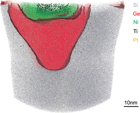
Semiconductor Devices
- Silicides
- High-k dielectrics
- Advanced metallization
- Channel engineering (Si/SiGe[B])
- Compound semiconductors
- 3D device structures
- Optoelectronics
3D Quantitative Metrology
Acquire useful information for the design, quality control and failure analysis of next-generation electronic devices, involving new materials (eg SiGe, doped nickel silicides, high-k dielectrics) and new 3D transistor geometries (eg finFETs).
Analyse Device Interfaces
With the CAMECA LEAP microscope you can characterise buried interfaces in 3D. For example, you can characterise local and interface composition to develop and ramp next generation device structures such as finFETs, as well as materials such as high-k dielectrics, contacts and high mobility channels. APT delivers 3D interface measurements not possible with other analytical techniques.
LEAP 5000 complements other methods such as TEM and SIMS, providing 3D compositional characterisation with nanoscale resolution.
Application Notes
These application notes are available to download from CAMECA:
- Correlative analysis – Carbon segregation with LEAP & STEM
- Grain boundary analysis – Analysis of Ni-based Super Alloy 600
- Grain boundary analysis – Analysis of Ultrafine Grained Light Alloys
- Nuclear – Nanoscale features providing radiation damage resistance
- Geology – 4.4 billion year old zircon
- Semiconductors – 3D analysis of a 28nm node S/D region
- LED device engineering – A case study in competitive analysis
- Optical fibres – LEAP analysis of dielectric nanoparticles
- Fuel cells – APT of perovskite materials
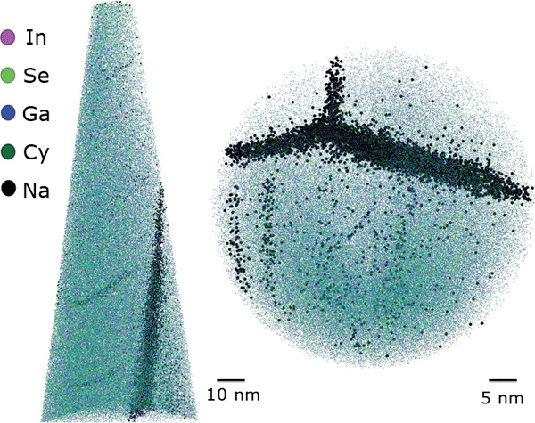
- Solar cells – Characterisation of buried interfaces in CIGSSe
- 3D FinFET – Sample prep & 3D analysis of a 14 nm Device
- Biological apatites – Interfaces and interphases in tooth enamel
- Synergistic t-EBSD/TDK & APT Grain Boundary Analysis
- Nanocluster Analysis – APT for Nuclear Structural Materials
- Correlative Grain Boundary Characterisation in the Local Electrode Atom Probe
- Optoelectronics: Dopant Distribution in ALD-grown ZnO
- Magnetic Thin Films for storage, memory & spintronics applications
- Paleoclimatology – Organic Matrices in Biogenic Carbonates
- Nanolaminates – Phase stability in Cu/Nb multilayered films
- APT-STEM Correlative Imaging for Enhanced 3D Reconstruction
The LEAP 5000 platform comes in three configurations:
LEAP 5000 XR
For all applications
- Ultra small spot UV laser pulsing capabilities
- Versatile model for a wide variety of applications
- Analyse complex, fragile materials
LEAP 5000 XS
Enhanced performance and throughput – for all applications
- Ultra small spot UV laser pulsing capabilities
- Highest sensitivity and throughput
- Largest analysis volumes
- Highest detection efficiency (80% of all atoms detected)
- Fastest analysis
LEAP 5000 R
For metals analysis
- Specifically designed for metallurgical applications
- Detects 50% of all atoms detected (40% more atoms per nm3)
- Improved compositional accuracy and precision and
high throughput - Most powerful voltage mode atom probe ever produced
Automation Packages
Automation packages are available for collecting data from large numbers of samples, and improving data quality and yield. Details are available in a brochure from CAMECA – contact us for quotes.