What is APT? (Atom Probe Tomography)
Atom Probe Tomography (APT) is the only materials analysis technique offering extensive capabilities for both 3D imaging and chemical composition measurement at the atomic scale.
Introduction to APT Webinar Series
Join CAMECA for a series of webinars in Autumn/Winter 2020 covering the basics of APT and its applications. Details and registration…
Blue Scientific is the official distributor for CAMECA APT instruments in the UK, Ireland and Finland. For more information or quotes, please get in touch.
CAMECA APT instruments
Contact us on +44 (0)1223 422 269 or info@blue-scientific.com
Follow @blue_scientific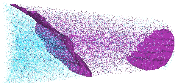
Atom Probe Tomography
Atom Probe Tomography (also referred to as APT or 3D Atom Probe) is the only materials analysis technique offering extensive capabilities for both 3D imaging and chemical composition measurements at the atomic scale (around 0.1-0.3nm resolution in depth and 0.3-0.5nm laterally). Even since its early development, Atom Probe Tomography has contributed to major advances in materials science.
- Single atom detection
- 3D tomographic data with near-atomic spatial resolution
- Equal sensitivity to all elements and their isotopes
- Quantitative composition measurement (sub-nm to micrometer scale)
How it Works
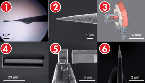
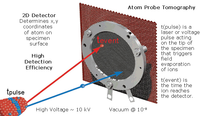
The sample is prepared in the form of a very sharp tip, with techniques very similar to TEM preparation. An atom probe produces images by field evaporating atoms from the specimen and projecting the resultant ions onto a detector. This results in the highest ion efficiencies of any 3D microscopy technique (up to 80%).
Data Collection
Atoms are identified by their mass-to-charge ratio using time-of-flight mass spectrometry. The detector simultaneously measures:
- Time Of Flight of the ions.
- X,Y position of the ion impact on the detector and their order of arrival, to record their precise original position with subnanometre resolution.
Data Visualisation and Analysis
By repeating this sequence, atoms are progressively removed from the tip and a 3D image of the material can be reconstructed at the atomic scale.
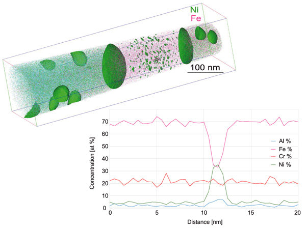
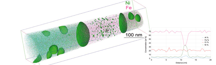
The resulting image shows the positions of individual atoms with subnanometre resolution. The reconstructed data set can be used for many types of useful analyses:
- 3D visualisation
- 2D atom mapping
- 1D depth profiling
- Line scanning
- Mass spectra
- Compositional analysis
Applications
APT can be used in a wide range of fields, including:
- Metals and alloys
- Coatings
- Thin films
- Ceramics
- Minerals
- Functional materials
- Additive manufacturing
- Semiconductors and microelectronics
- Geochemistry
Webinar Series
To provide an introduction to APT, CAMECA are presenting a series of webinars throughout Autumn/Winter 2020 covering various aspects of the technique and its applications.
Click the links below to register, and you’ll receive a link to attend. All webinars will take place at 10am CST:
Basics of APT
- Easy 3D Nanoscale Analysis – Watch on demand
- Specimen Preparation – Watch on demand
- Data Collection – Watch on demand
- Reconstruction and IVAS – Watch on demand
- Grain/Phase Boundary Analysis – Watch on demand
- Cluster/Precipitate Searching – 19th January 2021
Applications of APT
- Metals and Alloys – Watch on demand
- Nanomaterials – Watch on demand
- Wet APT Specimens – Watch on demand
- Geoscience – Watch on demand
- Semiconductors – 5th January 2021
- Dielectrics and Insulators – 2nd February 2021
- Nuclear Materials – 16th February 2021
APT Instruments
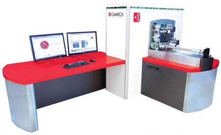
LEAP 5000
- Unmatched sub-nm performance.
- Collect nanoscale information from a microscale dataset in just a few hours.
- Large field-of-view and uniform detection.
- Optional cryo technology for life science and soft materials.
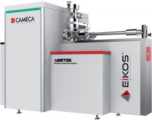
EIKOS-UV
- Routine 3D nano-analysis.
- For research and industry.
- Easy to site with a small footprint, requiring very few consumables.
More Information
Blue Scientific is the official distributor of CAMECA in the UK, Ireland and Finland. We’re available to provide quotes, advice and answer all your questions – just get in touch: