EIKOS
Atom Probe Microscope (APT) for routine 3D nano-analysis
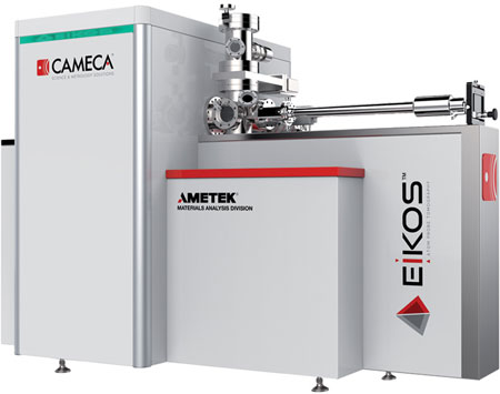
The CAMECA EIKOS is an atom probe microscope for rapid alloy development and nanoscale materials research.
- 3D tomography and nanoscale characterisation of microstructures
- Single atom detection at high spatial resolution
- Sensitive to all elements equally – including their isotopes
- Quantitative composition measurement (sub-nm to near micron scale)
- Configurations with voltage or voltage and laser
- Standard sample preparation techniques
What is Atom Probe Tomography?
Contact us for more information and quotes:
+44 (0)1223 422 269 or info@blue-scientific.com

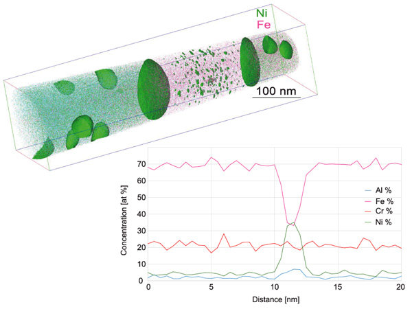
Atom Probe Tomography of an Iron-Based Superalloy

Grain Boundaries in Metals
The CAMECA EIKOS can characterise grain boundaries in materials studies, with nanoscale chemical analysis and 3D imaging. The functional properties of metals and alloys are often related to the chemical and morphological distribution of crystallographic grains in the material. The properties of the regions where grains come together (grain boundaries) can determine the formation, evolution and stabilisation (or dissolution) of the grains.
Phase Change Separation Processes
Due to its unique spatial resolution analytical capabilities, with sub-nanometre lateral and depth resolution, CAMECA Atom Probes are ideal for atomic scale quantitative analysis of materials.
APT is the only analytical technique that gives you both quantitative composition and atomic scale 3D elemental mapping of chemical heterogeneities. Similar to STM, you can image single atoms and their neighbours. However, APT has two significant advantages:
- Elemental analysis – Chemically identify each atom.
- Depth resolution – For 3D chemical maps.
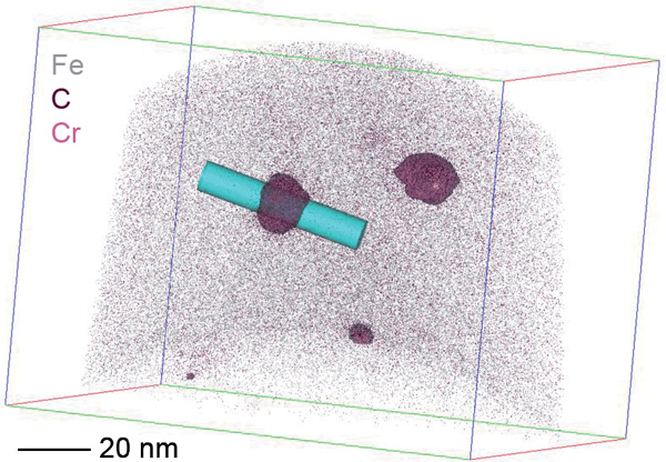
Nanoscale 3D Map of Stainless Steel

Application Notes
These application notes are available to download from CAMECA:
Two configurations are available:
EIKOS
Base system
- Reflectron design for excellent mass resolving power and signal to noise
- Pre-aligned integrated counter electrode for ease of use and reliability
- Voltage pulsing system
- Suitable for metallurgical applications
- Field upgradable to the EIKOS-UV
EIKOS-UV
Base system plus UV laser capabilities
- Includes all the features of the EIKOS base system
- Fully integrated 355 nm laser pulsing module
- PC-controlled focused spot design
- Full range of applications

