How Does a CMOS Camera Work?
Complementary metal-oxide semiconductor (CMOS) sensors are now one of the most widely used in camera technologies. Some of the advantages of CMOS technologies for camera sensors include their compact size, low-power draw, and generally cost-effective architectures.1
What makes CMOS sensors so space and power efficient is the integration of the electronics into the sensor itself. A typical CMOS camera is made of an array of photosensitive pixels. Each pixel contains a number of transistors that are made of a photodiode an amplifier.
When a photon hits the surface of the photodiode in the CMOS sensor, the material the photodiode is made of converts this to an electrical charge. The charge can then be converted to a voltage, amplified transmitted. As each pixel in a CMOS sensor has its own transistor, the pixel can be read out individually and without the need for any additional read-out electronics.
Key Attributes of CMOS Cameras
The lack of need for any additional read-out electronics is part of what makes CMOS sensors fast to read out and so compact in design. There are different shutter designs that can be used to either read out all pixels simultaneously, faster but with reduced image quality, or with a rolling shutter mode, where pixels are read out row-by-row avoiding the issue of continuous exposure and readout.
CMOS cameras can be used to capture light across many different regions of the electromagnetic spectrum, from visible light through to X-rays. In visible light applications, CMOS sensors can be combined with microlenses. With a microlens array, each lens is placed about the CMOS sensor to direct the light onto the sensitive part of the detector and increase the optical fill factor of the device. In the X-ray this is more challenging, as there are fewer optics that work in this wavelength regime to create the microlenses, but the CMOS sensor can still be used for direct X-ray detection.
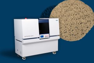
Introducing the Bruker Skyscan
The Bruker SkyScan is a high-resolution desktop micro-CT scanner (3D X-ray microscope). At the heart of this device is a 16 Megapixel CMOS Camera that allows for direct detection of the X-rays during imaging application.
The CMOS sensor in the Bruker SkyScan is what allows for super-efficient scan times with this instrument. Up to 5 times faster compared to conventional scanners that make use of a fixed camera position, the Bruker SkyScan capitalizes on the fast readout times of a CMOS camera for efficient scanning both in terms of image acquisition time but also in terms of optimizing scan parameters.
The Bruker SkyScan achieves its impressive acquisition times through the use of a feedback system with the CMOS sensor to set up automated scan parameters. This not only makes the device easy to use with fewer decision to be made by the operator but means the perfect combination of magnification, energy and filters are all selected for you, so you get the best imaging results every time.
The small size of the CMOS detector means the detector is easy to move and the CMOS camera can be positioned very close to the X-ray source. This helps avoid any intensity losses and ensure bright, clear images.
Contact us today to find out how the small-footprint Bruker SkyScan and its agile scanning capabilities with its high resolution CMOS sensor could benefit your application.
- Hellier, K., Benard, E., Scott, C. C., & Karim, K. S. (2021). Recent Progress in the Development of a-Se / CMOS Sensors for X-ray Detection. Quantum Beam Science, 5, 29. https://doi.org/10.3390/qubs5040029