Publication-ready data in minutes instead of hours.

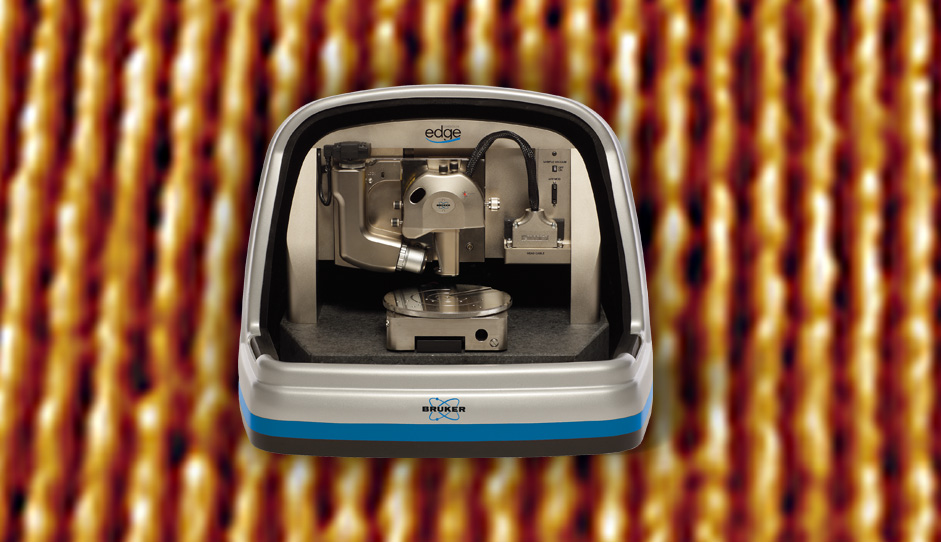
The Bruker Dimension Edge is the best value mid-range AFM. It uses the same technology as the Dimension Icon, with PeakForce Tapping for best-in-class performance on any AFM sample.
Publication-ready data in minutes instead of hours.
Modular microscope and electronics.
Motorised and programmable for multi-site measurements.
The Bruker Dimension Edge uses the same technology as the advanced Dimension Icon system, for impressive performance and functionality. Bruker’s revolutionary closed-loop tip scanner reduces positioning noise levels to the length scale of a single chemical bond.
Achieve consistent results quickly and easily with ScanAsyst automatic image optimisation technology. Designed to deliver the low drift and low noise necessary to achieve publication-ready data in minutes instead of hours, Dimension Edge is a best-in-class, powerful mid-priced AFM.
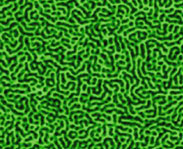
To design heterogeneous composite materials and utilise the huge variety of polymer chemistries and nanoscale building blocks, characterisation methods are needed that map properties at the highest spatial resolution. Micro-phase separations and the distribution of additives and fillers affect critical bulk properties, in applications from structural materials to organic photovoltaics.
The Dimension Edge provides a full suite of nano-mechanical and nano-electrical modes to fulfill these needs, ranging from phase imaging and force spectroscopy to piezo-response force microscopy, conductive AFM, and Kelvin probe force microscopy. All modes benefit from the highest spatial resolution, to easily achieve atomic resolution.
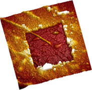
Electrochemical AFM (ECAFM) maps surface changes in situ, while the sample is immersed in the electrolyte and under electrochemical control. Applications include fundamental electrochemistry studies, corrosion and Li battery development.
Wide chemical compatibility with aqueous solutions as well as carbonate solvents (in the case of Li batteries) is key, necessitating the use of Teflon/Kel-F as cell material, sufficiently deep and sealable cup-shaped cells and imaging performance in liquid. Bruker’s dedicated electrochemistry cells are designed specifically to address these issues and provide turn-key solutions for Li battery research.
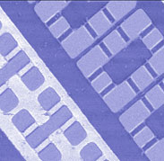
AFM-based nanoscale electrical characterisation is an established technique in semiconductor R&D, where scanning capacitance provides maps of active carrier density and conductive AFM probes device connectivity and gate oxide breakdown characteristics.
Nanoscale electrical properties are also important in other research areas, from graphene to conductive polymers, where the most useful AFM electrical modes are conductive AFM, Kelvin probe force microscopy (KPFM) and electric force microscopy (EFM). The Dimension Edge offers a full suite of electrical modes, with Bruker’s patented LiftMode for electric field gradient mapping with EFM, sensitive KPFM work-function mapping, and artefact-free conductivity mapping with Dark-Lift conductive AFM.
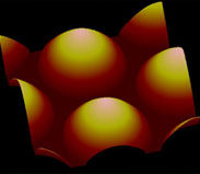
Patterned Sapphire Substrate (PSS) is used in LED manufacture, to enhance light output and efficiency. A PSS is typically a sapphire wafer, etched with a periodic pattern. The pattern can be conical, hemispherical or pyramidal. These structures are used to change the angle of outgoing photons, reducing total internal reflection to increase efficiency. Dimension Edge provides the metrology required to control the manufacture of PSS, including feature height, width and angle measurements, while also providing a full 3-D profile.