Excellent functionality and high resolution.
The Bruker Innova AFM delivers accurate, high-resolution imaging and a wide range of functionality for physical, life and material science research. The Innova is designed to be flexible and easy to use, as well as to fit your budget at a moderate cost.
Excellent functionality and high resolution.
With pre-configured software settings.
With TERS-enabled AFM-Raman integration.
The Innova features a unique, state-of-the-art closed-loop scan linearisation system for accurate measurement and noise levels approaching those of open-loop standard. Achieve atomic resolution and scans up to 90 microns, without changing scanner hardware. The integrated, high-resolution colour optics and programmable, motorised Z-stage make it quick and simple to find features and change tips or samples.
The Bruker Innova offers a complete choice of SPM techniques, for applications including photovoltaics, energy storage, surface science, device characterisation, biomolecules and semiconductors. A host of standard and optional scan modes enables complete surface characterisation of samples in both air and liquid.
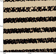
To design heterogeneous composite materials and choose from the wide range of of polymer chemistries and nanoscale building blocks available, it’s important to be able to map properties at high spatial resolution. In applications from structural materials to organic photovoltaics, critical bulk properties are affected by microphase separations and the distribution of additives and fillers. To address these characterisation needs, the Bruker Innova has a full suite of nano-mechanical and -electrical modes, from phase imaging and force spectroscopy to piezo-response force microscopy, conductive AFM and Kelvin probe force microscopy. This functionality is also offered by the Dimension Edge.
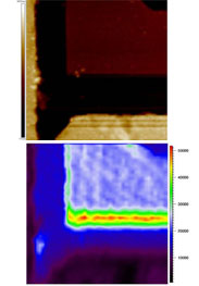
AFM-based nanoscale electrical characterisation is commonly used in semiconductor R&D and failure analysis. Scanning capacitance provides maps of active carrier density, and conductive AFM probes device connectivity and gate oxide breakdown characteristics.
Nanoscale electrical properties also play a key role in research areas from graphene to conductive polymers, using AFM electrical modes such as conductive AFM, Kelvin probe force microscopy (KPFM) and electric force microscopy (EFM).
The Bruker Innova offers a full suite of electrical modes, including:
AFM and Raman spectroscopy provide highly complementary information:
Combined AFM and Raman spectroscopy also facilitate tip-enhanced Raman spectroscopy (TERS), bringing Raman spatial resolution into the nano-scale. Innova (as Innova-IRIS) is an ideal platform for AFM-Raman and TERS, with stable hardware and software for integration.
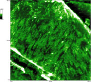
Analyse biological samples from single biomolecules to isolated membranes and whole live cells. The high resolution surface probe can work in-situ inside liquids, opening up life science application possibilities. Studies of live cells highlight cell responses to external stimuli. AFM research into isolated membranes reveals phase segregations and has even provided molecular-level detail structure and bonding informationn, for example on bacterio rhodopsin. Tapping mode in-situ AFM imaging and thermal-tune calibrated force spectroscopy of individual DNA and protein molecules can elucidate secondary structure and the potential energy landscape governing unbinding forces.