Characterising Photovoltaics and Solar Cells with Raman Spectroscopy
How Raman spectroscopy is used in the development of photovoltaics and solar cells, for research, development and quality control in manufacturing.
Blue Scientific is the official Nordic distributor of Renishaw Raman in the Nordic region (Norway, Sweden, Denmark, Finland, Iceland). For more information or quotes, please get in touch.
Renishaw Raman instruments
Contact us on +44 (0)1223 422 269 or info@blue-scientific.com
Follow @blue_scientificWhat can you study?
Raman spectroscopy can be used to characterise all photovoltaic materials, including Si-based, CIGS, CdTe, organics and III-Vs. You can study important material properties such as:
- Alloy fraction
- Electronic efficiency
- Strain/stress
- Thin film thickness
- Crystal structure type and orientation
- Crystal quality
- Sample uniformity and purity (eg defects and contaminants)
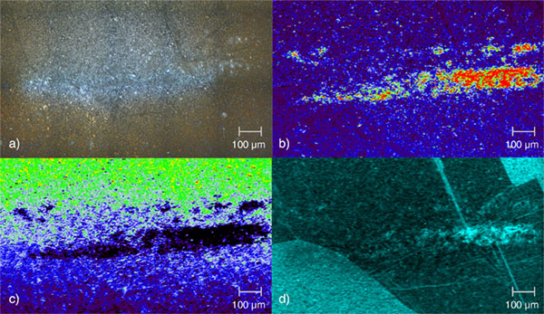
Discoloured polycrystalline solar cell (a). Raman images reveal changes in: (b) Silicon crystallinity at the discolouration points; (c) Stress around the discolouration regions; (d) Band intensity showing domain orientations and boundaries
Analyse Final Devices
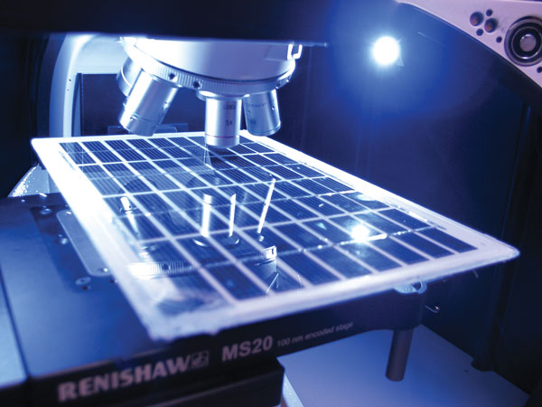
Complete devices can be studied, to analyse the effect of production processes on quality and performance.
Devices of all sizes can be measured, with a range of options and even custom solutions and free-space microscopes for the largest devices. This means that products of any size can be studied as complete modules in their finished state.
Study Variation in Material Properties
Study how material properties vary across the device with Raman imaging – extremely useful in photovoltaic development.
Renishaw Raman systems feature unique technologies for analysing both small and large areas, at a resolution that suits you. Build a picture of the device as a whole, not just isolated sections.
These large area modes are known as Streamline and Slalom:
- Streamline – Acquire high definition chemical images of large areas rapidly, with a line instead of a laser spot.
- Slalom – Fast scanning at lower resolution, for when you need quick results and the resolution’s less important. The laser line zigzags to ensure all details are included in the image.
Both techniques use the same lens for consistency, so you can compare images of different resolutions exactly.
More about Raman imaging and mapping
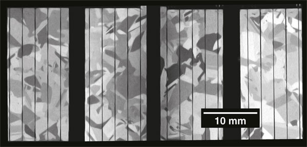
Raman image of crystal domains in a PV cell, taken using Streamline mode to image a large area. The size and shape of the domains indicates cell efficiency.
Switch Lasers Easily
It’s important to use the correct laser wavelength for your material, to avoid damage. Laser wavelength also affects the depth of analysis.
Renishaw’s inVia Raman microscope can be equipped with multiple lasers of different wavelength. You can then switch between them in seconds using the software.
Example: Perovskite Research
Perovskites (particularly hybrid organic-metal lead/tin halides) are promising solar cell materials, with advantages over crystalline silicon. Substrates can be coated from solution or by deposition to produce low-cost large-area cells. They can also be deposited on other cell types to create tandem cells with enhanced light-harvesting capabilities. However, they do have disadvantages, such as poor stability over time.
Raman spectroscopy is very useful for studying perovskites, because it delivers detailed composition and micro-structural information, and can identify degradation products. However, it hasn’t been adopted as widely because of issues with laser damage.
Renishaw presented a scientific poster on the subject, co-authored with researchers from the University of Sheffield and Swansea University. They experimented with various laser wavelengths from 488 nm to 830 nm, to find the most suitable for perovskite measurements.
Because the Renishaw’s inVia supports multiple laser wavelengths, you can easily select the optimum laser to maximise the signal while avoiding damage. Together with the use of a laser line rather than an intense spot, a higher power density can be used without damaging the perovskite.
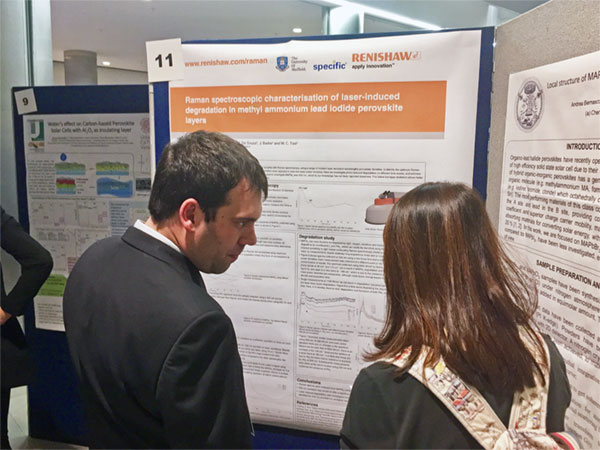
Tim Batten of Renishaw presents research using Raman spectroscopy at a perovskite solar cells conference.
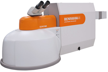
Renishaw Invia
A research-grade confocal Raman microscope:
- Outstanding performance and reliable results
- Easy to use
- Perform all types of Raman measurements
More Information
Blue Scientific is the official distributor of Bruker xxxx. We’re available to answer all your questions – just get in touch:


