+44 (0)1223 422 269 Contact

Posts Tagged ‘photovoltaics’

Silicon Wafer Defects

Characterising Semiconductors with Raman Spectroscopy

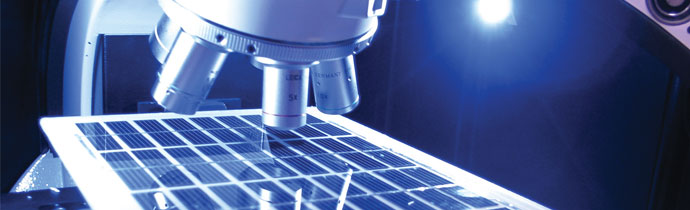
How Raman spectroscopy can be used to characterise semiconductor materials. Measure defects in SiC, crystal quality, stress/strain, homogeneity and more.

Raman Imaging Solar Cells & Photovoltaics

Characterising Photovoltaics and Solar Cells with Raman Spectroscopy

How Raman spectroscopy is used in the development of photovoltaics and solar cells.

Bruker PeakForce TUNA AFM

Nanoscale Electrical and Mechanical Property Mapping with AFM

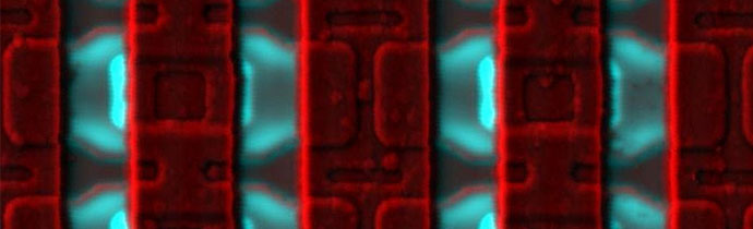
How to map current and conductivity at the nanoscale on fragile samples with AFM, without damaging them or contaminating the probe tip. Useful for lithium battery research, organic photovoltaics and carbon nanotubes.

EBIC (Electron-Beam Induced Current)

What is EBIC? (Electron-Beam Induced Current)

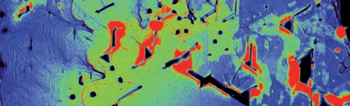
EBIC (Electron-Beam Induced Current) is a technique for characterising the electrical properties of semiconductor materials & devices. Reveal the subsurface electronic structure and analyse defects.

HOPV16 Hybrid and Organic Photovoltaics Conference – Swansea, 28/06/16-01/07/16

Visit us at HOPV16 on 28 June – 1 July 2016 in Swansea, and see the PhotoEchem with IPCE.