Complementary techniques for a wealth of data.

The Bruker Dimension Icon-Raman combines industry-leading AFM together with a research-grade confocal Raman microscope in a single instrument.
Combining Raman spectroscopy with Bruker’s Dimension Icon platform gives you high performance surface characterisation with easy and efficient co-localised measurements. These complementary technologies provide critical information about the sample’s topography and chemical composition.
Gain unique insights into the mechanisms that lead to specific material properties, with advanced AFM modes including electrical characterisation and quantitative nanomechanical mapping.
Complementary techniques for a wealth of data.
Correlated instantly.
Plus spectroscopic methods.
The Dimension Icon-Raman incorporates the Bruker Dimension Icon AFM and a research-grade confocal Raman microscope (Horiba, LabRam) on a single, rigid, anti-vibration platform. Each instrument retains its full functionality, with all original features for optimum combined performance.
This includes all Bruker Icon upgrades and AFM modes, including their exclusive ScanAsyst self-optimising technology. Tailor the most effective combination of modes for your application. We are available to advise on which options would be best to achieve the results you need.
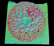
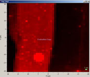
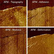
With combined measurements, the sample is transferred between the two techniques in seconds via a high-precision X-Y stage. AFM and Raman measurements are carried out consecutively. Raman mapping and imaging results are correlated easily with AFM images using Bruker’s powerful microscopy overlay software, MIRO. Stacks of data sets (topography, modulus and adhesion maps) can be overlaid with a chemical distribution map, resulting in comprehensive, correlated information.
With a full complement of techniques, advanced features and µ-Raman capabilities, the Dimension Icon is ideal for advanced research into the mechanisms underlying the effect of chemical composition or crystalline structure on material properties.

AFM and Raman microscopy data is highly complementary, providing useful insights into materials and polymer samples:
Correlating these two techniques connects chemistry with function, for example to highlight the most conductive components in a device, or to measure stiffness in structural materials.

In heterogeneous polymer samples, correlating AFM and Raman maps is very useful, because chemistry often affects properties. Once the Raman map has identified the chemistry of the sample’s micro-phases, the AFM property map can be used as a higher resolution chemistry map. PeakForce QNM (Quantitative Nanoscale Mechanical Characterisation) mode can be used to produce property maps with high spatial resolution, that are unambiguous, quantitative and highly reproducible. Produce chemistry maps in your lab with nanometer spatial resolution.

Bruker Atomic Force Microscopes are widely used in materials science and polymer research labs. AFM is ideal for research into the nanoscale properties of nanocomposite materials. Bruker’s exclusive PeakForce QNM(Quantitative Nanoscale Mechanical Characterisation) mode rapidly maps nanomechanical properties including modulus in high resolution over a wide range (kPa to GPa). Most Bruker AFMs are also available with high temperature heating and cooling options, which can be used to investigate polymer phase transitions, as well as many other applications. The full range of techniques includes thermal analysis, electrical property mapping (current and capacitance) and nanoindentation – please contact us for details.

PeakForce QNM mode maps of nanomechanical properties including modulus in high resolution over a wide range (kPa to GPa). Modules for specific applications enables electrical measurements including current mapping (conductive AFM), low current mapping (“Tunneling AFM”, TUNA) and wide range current measurements (Scanning Spreading Resistance, SSRM). Bruker’s exclusive PeakForce Tapping technology and PeakForce TUNA mode combine superior force control and nanomechanical property mapping with high current sensitivity. High resolution surface potential mapping is also possible, with higher sensitivity than ever before.
With Renishaw's new Correlate software module, you can combine results from various microscopy techniques for more powerful data.
How to combine Atomic Force MIcroscopy (AFM) and Raman spectroscopy for enhanced nanoscale information about your sample's structure, composition and properties.