What is 4D STEM?
4D STEM is an electron microscopy technique that captures a full 2D diffraction pattern at each pixel position on a STEM (Scanning Transmission Electron Microscopy) map. Here’s an overview of 4D STEM techniques, including:
- Virtual imaging
- Orientation mapping
- Strain mapping
- Differential phase contrast
Blue Scientific is the official Nordic distributor for Gatan in Norway, Sweden, Denmark, Finland and Iceland. For more information or quotes, please get in touch.
Gatan STEMx
More articles about TEM / SEM
Contact us on +44 (0)1223 422 269 or info@blue-scientific.com
Follow @blue_scientificWhat is 4D STEM?
4D STEM is an electron microscopy technique that captures a full 2D diffraction pattern at each pixel position in a STEM (Scanning Transmission Electron Microscopy) map.
In STEM, diffracted signals are extremely rich in information. They containing localised data about a material’s structure, composition, phonon spectra, 3D defect crystallography and more. Conventional STEM imaging records only one or two values per probe position, ignoring most of the diffracted signal information. With new high-speed direct electron detector technology, a full image of the diffracted electron probe can now be recorded at each position, producing a four-dimensional dataset.
4D STEM has also been known as:
- Position resolved diffraction (PRD):
In early experiments using a 2D scan instead of a line scan. - Spatially resolved diffractometry:
In virtual imaging. - Pixelated STEM
- Scanning electron nanodiffraction or nanobeam electron diffraction (NBED):
Usually when a nanometre-scale beam is used. - Momentum-resolved STEM:
Another name for 4D STEM, because it involves real- and momentum space data.
There are also several terms used to refer to electron diffraction patterns produced using a converged (STEM) probe:
- Convergent beam electron diffraction (CBED)
- Microdiffraction
- Nanodiffraction
- Diffraction imaging
How it Works
In STEM, the electron beam is focused on an electron transparent specimen to make a probe from a few nanometres down to nearly atomic dimensions. Electrons interact with the specimen, and once they are scattered, different types of signals can be measured:
- X-rays (EDS)
- Back-scattered electrons
- Light (cathodoluminescence)
- Auger electrons
- Secondary electrons
- Inelastically scattered electrons (energy loss spectroscopy)
- Elastically scattered electrons (diffraction)
Conventional STEM detectors record a single value per probe position. In 4D STEM, the probe is rastered on the specimen in a 2D array. At each probe position, a 2D diffraction pattern is imaged on a pixelated detector. This generates a 4D data cube that can then be analysed further.
Video courtesy of Colin Ophus, Molecular FoundryVirtual Imaging
One of the key applications of 4D STEM diffraction is virtual imaging. This involves generating:
- Virtual selected area diffraction image
Sum the diffraction images from multiple real space probe positions (pixels) in the 4D data cube. - Virtual bright/dark field image
Apply a formula (eg sum, subtract) to the intensities of a subset of pixels in the diffraction domain. This value is then assigned to corresponding pixels in the virtual image.
Virtual imaging has several benefits:
- Use geometry and STEM detector combinations that would be impossible to create in a real microscope.
- Use any relative angular range and number of STEM detectors simultaneously.
- Higher signal to noise ratio images.
- Less affected by specimen bending and dynamic scattering (more details in this paper in Ultramicroscopy).
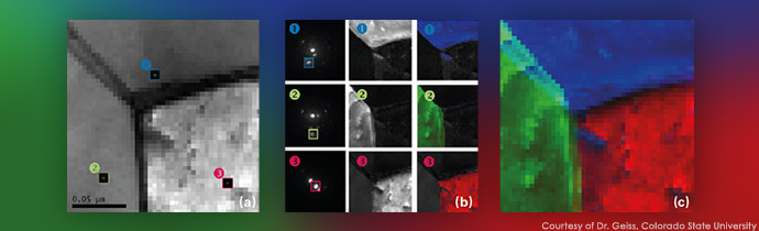
Orientation Mapping
Orientation can be mapped at higher resolution with 4D STEM – just like with EBSD (Electron Backscatter Diffraction) in a SEM. There are two techniques for this:
- Fitting Kikuchi diffraction patterns
For thick specimens, but sometimes fails in areas with high local deformation. - Diffraction spot indexing
For thinner specimens, using a template matching method. The process can be automated.
Strain Mapping
The mechanical and electrical properties of materials are directly related to their local atomic spacing (strain). There are two ways to measure strain using 4D STEM:
- CBED (Convergent Beam Electron Diffraction)
Higher-order Laue zone (HOLZ) features are measured by rotating the sample into a certain orientation. - NBED (NanoBeam Electron Diffraction)
Based on the inverse relationship between atomic distances and diffraction spots.
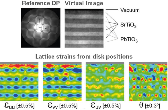
In the example below, as the crystal expands, the diffraction pattern contracts and vice versa. As well as crytalline materials, 4D STEM can also be used for strain measurements on amorphous and semi-crystalline materials.
Differential Phase Contrast
For a long time, fixed segmented STEM detectors have been used to measure electron beam deflection and correlate it to the sample’s electric field (electrostatic potential gradient). With this technique, information transfer efficiency is limited over several spatial frequencies.
4D STEM overcomes this limitation by measuring the movement of the center of mass (COM) of the bright field disc at each pixel position and calculating the electric field using COM displacement vector maps. Differential Phase Contrast provides images that can be directly interpreted as the (projected) electrostatic potential of a thin specimen. This makes it possible to image low-z elements – unlike HAADF imaging or Z-contrast imaging, which is better for elements with high scattering power.
Recorded Webinar
In this 1 hour recorded webinar from Gatan, Colin Ophus of the Moelcular Foundry at Berkeley Lab discusses the challenges and opportunities created by 4D STEM, and the experiments that are now possible with high-speed direct electron detectors:
Instrumentation
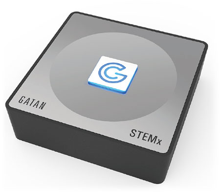
STEMx
- Enhance the capabilities to Gatan in-situ TEM cameras with 4D STEM.
- Fast results in <10 minutes.
- Handles large datasets easily.
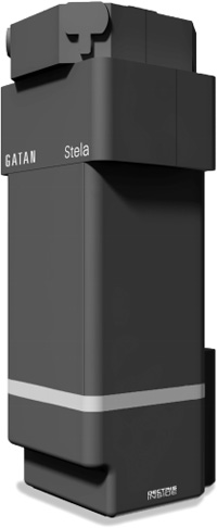
Stela
- Hybrid-pixel camera with STEMx.
- Complete, integrated system for 4D STEM.
- Works seamlessly with Gatan Microscopy Suite.
- Ideal for materials requiring low kV imaging (<80kV).
More Information
Blue Scientific is the official distributor of Gatan systems for electron microscopes in the Nordic region. We’re available to answer all your questions – just get in touch: