Gatan’s best-in-class BioContinuum imaging filter for cryo-EM is now available with EELS and EFTEM.
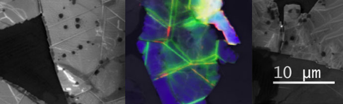
Cathodoluminescence can be used to study crystal structure orientation – in this example we look at how it can be used on a geological sample.

The Thermo Scientific Phenom Pharos G2 is a desktop FEG-SEM (Field Emission Gun – Scanning Electron Microscope) with upgraded features and low kV imaging.
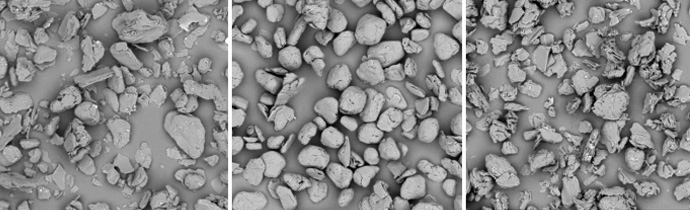
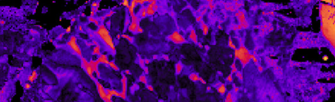
How desktop SEM can used in-house in lithium ion battery development to analyse graphite and battery materials.
BlueScientific is now the official UK distributor of Phenom entry-level SEM instruments from Thermo Scientific in the UK and Ireland. We now offer the most comprehensive entry-level range for industry QC and academic research: the fastest and highest resolution in their class.

A new fully-integrated system from Gatan and DECTRIS provides low-voltage capabilities for electron counting on EELS, EFTEM and energy-filtered 4D STEM over the entire 30 – 300 kV voltage range.
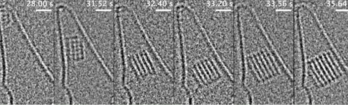
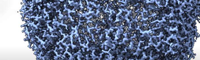
Capture dynamic processes during in-situ TEM experiments with the Gatan OneView IS camera, at up to 25 fps with 16 MP images. In this example, researchers at the University of Tokyo observed crystal nucleation and growth at atomic scale.
Register now for MMC 2021 (online) microscopy conference. Visit our virtual booth at the exhibition!