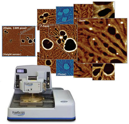
Electrical AFM Techniques – Bruker NanoElectrical Lab
Bruker NanoElectrical Lab is a comprehensive package of electrical AFM techniques, with new DataCube modes. The new nanoelectrical AFM modes give you complete materials characterisation, with more information about your sample than was previously possible. By correlating mechanical and electrical data at each pixel, you can gain a deeper understanding of a material’s properties.
These modes can be used with Bruker’s Dimension FastScan and Dimension Icon AFMs.
Blue Scientific is the official distributor for Bruker AFM in the Nordic region (Norway, Sweden, Denmark, Finland and Iceland). For more information or quotes, please get in touch.
Bruker AFM
Contact us on +44 (0)1223 422 269 or info@blue-scientific.com
Bruker NanoElectrical Lab
Bruker’s NanoElectrical Lab is a new package of AFM modes. Going beyond conventional electrical modes, they correlate electrical and mechanical information into multi-dimensional data cubes.
For materials scientists and engineers, this takes you beyond the usual limitations of efficiency and characterisation. You can now capture nanometre-scale electrical and mechanical characteristics simultaneously, in high-density data cubes – previously this was not possible from a single measurement.
Acquire Data Simultaneously
DataCube mode acquires a force-distance spectrum at every pixel. Electrical measurements are performed during a specified dwell time. This gives you electrical and mechanical spectra at every pixel.
Typical force-distance spectra, with a ramp rate of 40 Hz and a 100 ms dwell time per pixel, provide full characterisation from just one single experiment. This is unprecedented in a commercial AFM.
Previously, rendering topographical, mechanical, and multidimensional electrical information simultaneously would have been a monumental task. Now it can be performed as a routine AFM measurement.
The new modes render multidimensional data cubes at nanometre scales, with compound data in every scan.
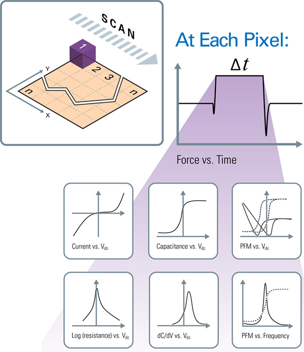
Acquire topographical, mechanical and multidimensional electrical information simulatenously at every pixel
New Modes
DataCube-TUNA
With DataCube-TUNA mode you can simultaneously acquire nanomechanical information and electrical conductivity at multiple sample voltages in a single measurement. This gives you a dense data cube of information.
Varying the sample voltage influences conductive AFM results, giving you insights into the performance of a material or device. This is the only mode that delivers a complete picture of:
- Sample conductivity
- Conductivity type (eg Ohmic, non-Ohmic, Schottky)
- Barrier heights
Current images of Maghemite (γ-Fe2O3), ramping the sample voltage from -2V to +2V at each pixel. Different grains have varyius conduction mechanisms, shown by viewing the data as ‘slices’ by sweeping the voltage.
DataCube-SSRM
Scanning Spreading Resistance Microscopy (SSRM) maps variations in majority carrier concentration in doped semiconductors.
With this mode you can acquire nanomechanical information and 3D carrier density maps simulataneously, from just one measurement. This gives you a data cube for complete characterisation, including:
- Nanoscale topography
- Mechanical information
- Log-resistance spectroscopy
- I-V measurements for conductivity eg Ohmic, non-Ohmic, Schottky, etc
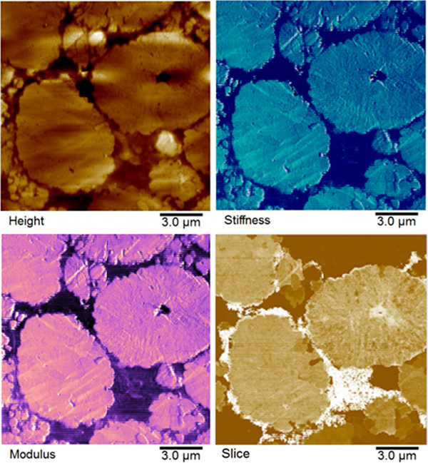
Correlated data on a Li battery cathode, taken using DataCube-SSRM. This shows large, hard grains of metal oxide, surrounded by carbon black particles with low resistance and soft, non-conducting polymer mediating the volume change during charging cycles.
DataCube-SCM
Scanning Capacitance Microscopy (SCM) measures active carrier concentration, with nanometre-scale accuracy. This mode acquires nanomechanical and carrier information simulataneously, at multiple sample voltages.
With DataCube SCM you can study dC/dV amplitude, dC/dV phase value changes and junction position shifts. The data cube gives you information about:
- Oxide thickness
- Oxide charges
- Threshold voltages
- Contamination from mobile ions
- Interface trap density
dC/dV amplitude images collected on two adjacent pnp transistors in SRAM memory, with the sample voltage ramping from -2V to +2V. The voltage-dependent pn junction positions corresponds to the expected behaviour. Some dopant defects are only visible at specific voltages. Scan size 3×3 um. Courtesy of N. Chevalier & D. Mariolle, Uni. Grenoble Alpes, CEA, LETI, France.
DataCube-PFM
Piezoresponse, or Piezoforce Microscopy (PFM) maps inverse piezoelectric effects at nanometre scale.
DataCube-PFM simultaneously collects nanomechanical information and PFM amplitude/phase spectra. The data cubes show the switching voltage of each individual domain, all in one data set.
This is performed without the usual drawbacks of conventional contact mode techniques, such as artefacts, sample damage and complicated data analysis.

Left: DataCube-PFM height & PFM images; Right: Spectra plots along a 1.2 µm line across multiple domains in a BFO ferro-electric sample. The plots show both PFM amplitude and PFM phase vs. bias during a ramp of -6V to 0V. The switching voltage can be extracted for each domain. (Click to enlarge)
DataCube-CR-PFM
DataCube-CR-PFM combines piezoresponse/piezoforce microscopy with contact resonance.
This gives you the benefits of DCUBE-PFM together with a frequency ramp at every pixel. This includes a full spectrum and peak sensitivity at the contact resonance.
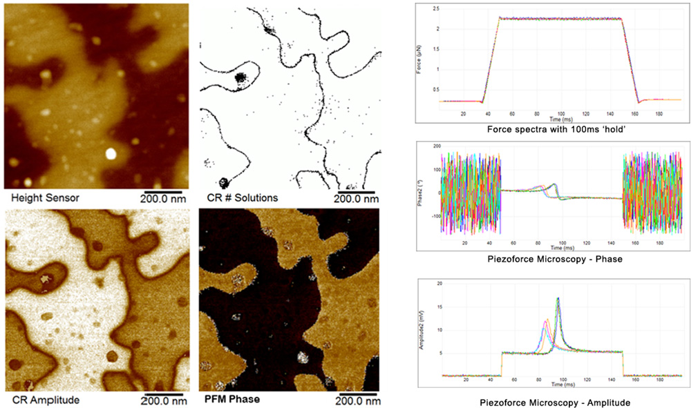
DataCube-CR-PFM data from LiTaO3 showing topography, PFM amplitude at contact resonance, PFM phase and the number of CR peaks (zero if there is no piezo-electric response). Example PFM amplitude & phase vs. frequency spectra, and corresponding force spectra are shown for a few pixels. Click to enlarge.
DataCube-sMIM
Scanning Microwave Microscopy Imaging (sMIM) maps the capacitive (C ) and resistive (R) impedance, as well as dC/dV, and dR/dV data – at a specified sample voltage.
With DataCube-sMIM you can study the same properties at various sample voltages. Just one scan is enough to give you the whole picture. The spectra also provide information such as:
- Conduction type (eg Ohmic, non-Ohmic, Schottky, etc.)
- Oxide thickness
- Oxide charge
- Contamination from mobile ions
- Interface trap density
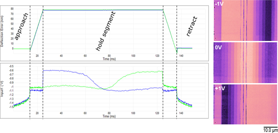
Force vs. time, and Capacitance (sMIM-C) vs. time plots for 2 pixels with opposite dopant types. The typical S-shaped C-V curves, acquired with a 100ms dwell time, are visible for both n-type and p-type. The images show ‘slices’ at 3 sample voltages on a Si sample with dual staircase profile. The contrast & sensitivity in n-type and p-type regions varies with the voltage. Click to enlarge.
Techniques and Applications
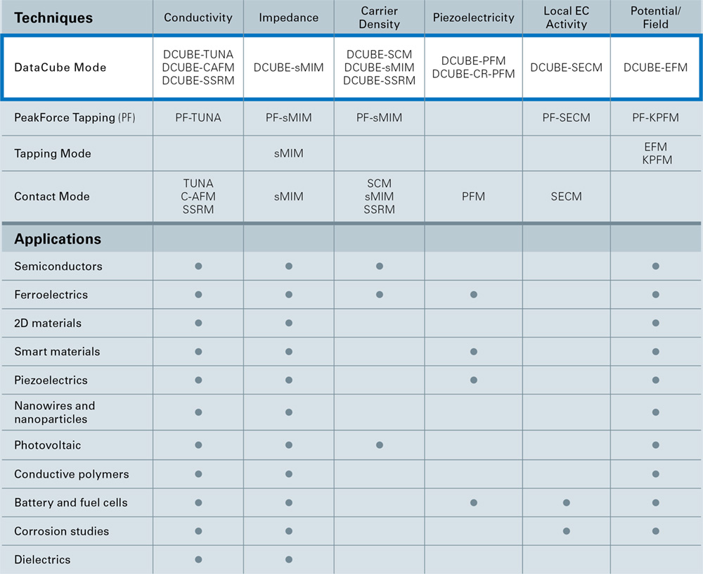
Click to enlarge
The new modes can be used with Bruker’s Dimension FastScan and Dimension Icon AFMs:
For further information please get in touch:
Contact us on +44 (0)1223 422 269 or info@blue-scientific.com
Bruker AFM


