How Raman spectroscopy can be used to characterise semiconductor materials. Measure defects in SiC, crystal quality, stress/strain, homogeneity and more.

How nanoscale infrared spectroscopy can be used to measure semiconductor materials in defect and contamination analysis, and fabrication.
How to combine Raman and nanoindentation for correlated mechanical and chemical data, delivering insights into your material’s properties.
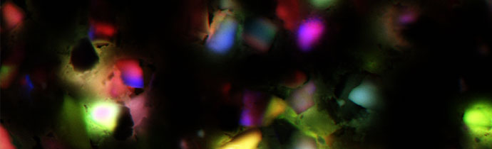
Cathodoluminescence (CL) is a technique for characterising composition, optical and electronic properties with data that correlates with morphology, micro-structure, composition and chemistry at the nanoscale.