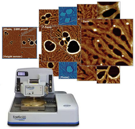
Nanoscale Electrical and Mechanical Property Mapping with AFM
How to perform high resolution current mapping on fragile samples. Study conductivity on organic photovoltaics, conductive nanotubes and nanoparticles without damaging your sample or contaminating the probe tip.
Blue Scientific is the official distributor for Bruker AFM in the Nordic region (Finland, Denmark, Sweden, Norway & Iceland). For more information or quotes, please get in touch.
Bruker AFM
PDF application note
Contact us on +44 (0)1223 422 269 or info@blue-scientific.com
Quantitative Electrical Property Measurements
Conventional AFM techniques have not been able to measure electrical properties quantitatively at the nanoscale. This is important in many fields, including solar energy, photovoltaics, OLED and other electrical devices. Bruker’s PeakForce TUNA AFM mode overcomes previous limitations, delivering both high resolution and quantitative characterisation at the nanoscale
Standard AFM conductivity mapping uses contact mode techniques, with lateral forces that can damage your sample and cause tip contamination. This limits the spatial resolution and results in artifacts that obscure your data. PeakForce TUNA overcomes these limitations with direct, accurate force control without any lateral forces.
Nanoscale Mapping
PeakForce TUNA uses Bruker’s proprietary PeakForce Tapping high resolution AFM technology for the most complete and highest resolution property mapping currently possible. With PeakForce TUNA you can map conductivity quantitatively on fragile samples, including organic photovoltaics, lithium ion cathodes and carbon nanotube assemblies, without sample damage or tip contamination.
- Highest resolution current mapping – even on fragile samples
- Nanoelectrical measurements with unmatched repeatability and consistency
- Correlated nanomechanical and nanoelectrical properties
Advantages of PeakForce TUNA
Peakforce TUNA gives you current imaging with the highest sensitivity together with high spatial resolution on fragile samples, while simultaneously acquiring correlated mechanical property data at each location.
- PeakForce Tapping technology for high resolution
- Powerful current amplifier:
- High bandwidth (>10kHz for 1010 V/A stage)
- Low noise (<100fA, cycle averaged, imaging bandwidth)
- Full fA to µA current range without changing the module or probe holder
- Self-optimising ScanAsyst features so you can acquire high quality results easily
- Highest resolution quantitative nanomechanical property mapping (PeakForce QNM)
Applications
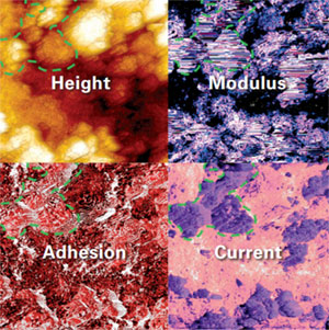
Simultaneous nanomechanical and
nanoelectrical property mapping on a Lithium ion cathode (L333). Courtesy of Dr. Battaglia, LBL.
Lithium Batteries
Cathode composite formation dramatically affects Lithium battery performance. Studying nanoscale phase separation and local electrical properties can help optimise processing conditions.
In this example from an L333 glue composite, there is a clear correlation between Young’s modulus, adhesion and current maps. You can assign materials and determine their dispersion. Analysis revealed a conductive network in the PVDF+AB region with a coverage of 56%.
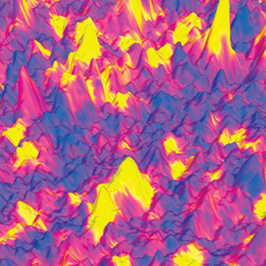
High resolution conductivity map of organic photovoltaic overlaid on topography. Courtesy of Prof. Nguyen, UCSB.
Organic Photovoltaics
PeakForce TUNA can also be used in research to improve the energy conversion efficiency of organic photovoltaic materials (OPVs). Due to their bulk heterojunction structure, their efficiency depends on the interfacial charge separation (exciton dissociation), as well as transport along nanoscale conductive pathways, due to nanoscale phase separation.
This example is a high resolution conductivity map of PEDOT-P3HT. Local current maxima (yellow) indicate partially sub-surface conductive networks. The current range is 5pA, height range 10nm, with a 2µm image size .
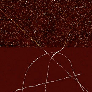
Height (top) and current (bottom) maps showing electrical connectivity on fragile carbon nanotube sample. Courtesy of Prof. Hague, Rice University.
Carbon Nanotubes
A growing area of research is nanoscale building blocks, such as carbon nanotubes. They are notoriously difficult to image with conventional AFM, because of their sensitivity to lateral forces.
This example shows topography and current maps from a carbon nanotube. By studying conductivity for individual carbon nanotubes, you can understand their state of electrical connectivity with a macroscopic electrode.
Instrumentation
PeakForce TUNA is available on these Bruker microscopes:
![]()
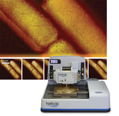
Dimension FastScan
World’s fastest AFM
More info…
Dimension FastScan Bio
Advanced biological AFM
More info…
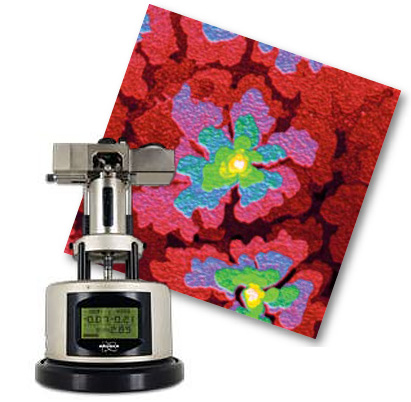
Dimension Icon
Flexible, large sample AFM – try it out at our Nordic SPM Conference!
More info…
![]()
Further Information
Blue Scientific is the official Nordic distributor for Bruker AFM. If you have any questions of if you’d like a quote, please get in touch:
