What is EBIC? (Electron-Beam Induced Current)
EBIC (Electron-beam induced current) is a microscopic technique for characterising the electrical properties of semiconductor materials and devices. Study the subsurface electronic structure and analyse defects.
The Gatan SmartEBIC is a complete system for EBIC experiments using a SEM or STEM microscope.
Blue Scientific is the official distributor for Gatan systems for electron microscopes in the Nordic region (Norway, Sweden, Denmark, Finland, Iceland). For more information or quotes, please get in touch.
Gatan instruments
Contact us on +44 (0)1223 422 269 or info@blue-scientific.com
What is EBIC?
Electron-beam induced current (EBIC) is a technique for analysing the electrical properties of semiconductors. EBIC involves measuring the electrical current that flows when a sample is exposed to an electron beam.
Any variation in the generation, drift or recombination of the charge close to the generation volume can be measured as contrast. This reveals the local, sub-surface electronic structure of the material or device. It’s a powerful technique for characterising defects and their effects in materials and devices. For standard EBIC, no bias is required.
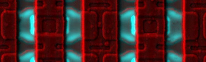
EBIC image showing the electrical activity of grain boundaries in CdTe solar cell. Courtesy of Dr. J. Poplawsky, Oak Ridge National Laboratory.
How it Works
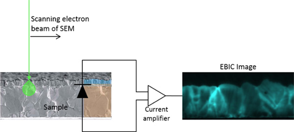
EBIC involves measuring the electrical current that flows when a sample is exposed to an electron beam.
When the electron beam meets the semiconductor, it creates electron-hole pairs. If the carriers of these pairs diffuse into a region with a built-in electric field, the electrons and holes separate and a current flows. EBIC measures this current as it joins an external circuit.
In a material with no recombination centres (places where the free electrons and holes annihilate) the current is uniform and therefore of little interest. However, where electrons and holes recombine, the current is reduced. This creates contrast in an EBIC map, highlighting the flow of (minority) carriers in the semiconductor.
How EBIC works
EBAC
Electron-beam absorbed current (EBAC) is a related technique that shows the local resistance of a sample. This is useful for identifying breaks in copper lines in electronic devices, as well as shorts and breakdown channels in capacitors.
EBAC involves measuring the absorbed current that flows between an electron beam and an electrical probe. The current measured in the external circuit is proportional to the resistance of the electrical path.
Advantages of EBIC
- Assess uniformity in device fabrication – Examine p-n junction and depletion region locations
- Optimise processing techniques – Build more effective devices, by understanding the effects of recombination centres eg grain boundaries, dislocations and precipitates
- Evaluate the quality of materials – Measure minority carrier diffusion lengths
- Locate faults quickly – Identify line breaks in integrated circuits
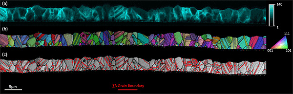
EBIC image using thermal representation of a defect in Si photovoltaic.
Step-by-Step Workflow
Step 1: Sample Preparation
Many devices including solar cells, laser diodes and transistors require no sample preparation. For standard EBIC, the sample needs:
- An electrical junction with diode characteristics, to provide an electric field to separate electrons and holes.
- Ohmic contacts to connect to an external circuit.
To study a material before device fabrication, a diode junction can be created by depositing a thin, electron transparent, metallic Schottky barrier character on the region of interest and a second ohmic junction that can connect to the external circuit.
Step 2: Load the Sample and Check Electrical Contact
Both EBIC and EBAC involve measuring small currents, so electrical contact is necessary. Specific EBIC sample holders have wire bonding for this purpose, or you can use micromanipulators.
Usually a current-voltage trace is used to asses the diode characteristics and decide whether the sample is suitable. For quantitative EBIC, the leakage current in reverse bias and shunt resistance should be low.
The EBIC holder can be loaded onto the stage using the load lock of the SEM. The stage can be modified to include connections for the EBIC or EBAC signal pass to the external circuit for measurement. An IV trace is used to check the contact.
Step 3: Imaging
The electron beam is scans in an X,Y pattern, measuring the current at each pixel. The magnitude of the current is displayed on the map in greyscale: small current in black and larger currents in white.
Qualitative imaging highlights electrical junctions, and quantitative analysis gives you more information. On quantitative maps, the greyscale levels indicated measured currents (usually in the pico- to micro-A range), rather than arbitrary units. This is useful when comparing materials, and understanding the extent and effect of defects.
Step 4: Analysis
Electrical properties can be measured in absolute intensity current values. EBIC contrast is even more useful when studying the extent of defects, eg dislocations, grain boundaries and stacking faults. This involves measuring the current normalised by the background signal, which correlates directly with the defect’s recombination strength.
You can also study local minority carrier diffusion lengths, by analysing the EBIC profile of the diffusion of minority carriers to an electrical junction.
[hr]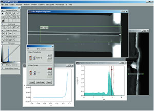
Gatan SmartEBIC
- Use with SEM or STEM microscopes
- Automatic routines and calibration for high quality results
- Includes beam control system, sample holders, cabling, connections and Gatan’s Digital Micrograph software
Further Information
Blue Scientific is the official Nordic distributor for Gatan, and we’re available to answer all your questions about EBIC and how it would suit your area of work.
More detailed information about the technique is also available in this pdf from Gatan:
Application Note
Gatan instruments
Contact us on +44 (0)1223 422 269 or info@blue-scientific.com