Characterising Semiconductors with Raman Spectroscopy
An overview of how Raman spectroscopy can be used to characterise semiconductor materials for electronics, transistors, solar cells, light emitting diodes and more.
Blue Scientific is the official distributor for Renishaw Raman in Norway, Sweden, Denmark, Finland and Iceland. For more information or quotes, please get in touch.
Renishaw Raman instruments
Contact us on +44 (0)1223 422 269 or info@blue-scientific.com
Follow @blue_scientificCharacterising Semiconductors
Raman spectroscopy is ideal for studying semiconductor materials in electronics, transistors, solar cells, light emitting diodes and more. It’s a powerful analytical technique, well suited to characterising the homogeneity of source materials, to perform in demanding semiconductor applications.
Characterising Photovoltaics and Solar Cells with Raman Spectroscopy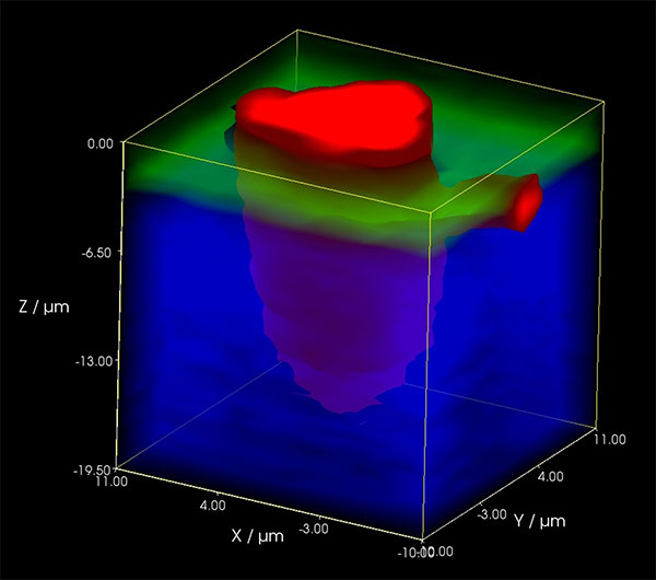
What Can You Measure?
With Raman you can generate images and characterise all types of semiconductors, including Si, carbon-based, III-V’s and polymers, as well as superconductors. This provides a wealth of information, including:
- Chemical composition eg alloy fractions of compound semiconductors
- Polytypes eg 4H-SiC and 6H-SicC
- Stress and strain
- Dopant concentrations
- Thickness of thin films
- Crystal structure type and orientation
- Crystal quality
- Defects
- Uniformity and purity
- Device temperature
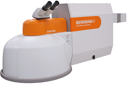
Renishaw inVia
A research-grade confocal Raman microscope ideal for measuring semiconductor materials.
- Perform all types of Raman measurements
- Flexible system – choose the optimum laser, optical components and accessories for your work
- Automate common tasks to save time
Convenient and Easy to Use
Raman is a convenient technique to use, making it a practical option for your lab. There’s no sample preparation, and vacuum technology is not required. In addition to this, there are no troublesome charging effects to deal with.
Renishaw Raman systems can be tailored to suit users of various experience levels, from technicians to research scientists.
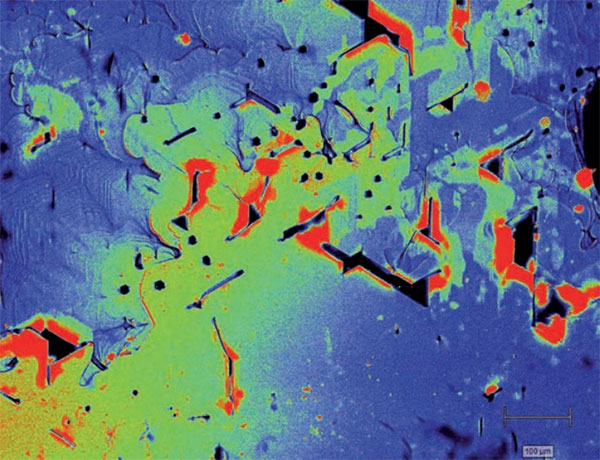
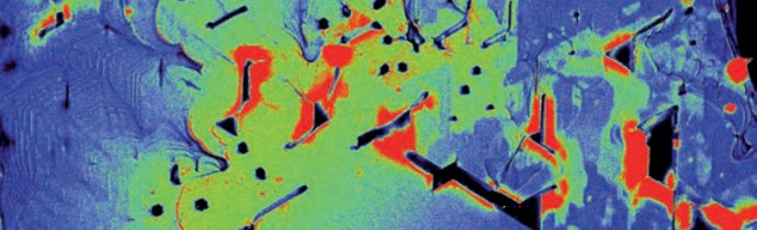
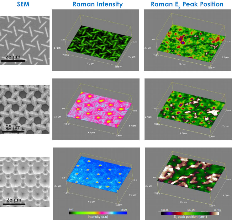
Analyse Large Areas
Renishaw Raman systems can analyse very large samples. This means you can generate images of entire wafers to locate contaminants or residual stresses.
Using a highly accurate, motorised stage, the sample is moved extremely precisely to acquire large images without the artefacts associated with tiling.
More about large area mappingPhotoluminescence
You can also collect and analyse photoluminescence spectra (PL), which augment the Raman data. Both vibrational and electronic information can be collected using a single instrument.
PL can be used to examine crystal defects, such as atomic vacancies and substitutions. This is partiularly significant for materials such silicon carbide. As well as identifying the defect, you can also tell if the crystal has internal stresses.
Compound Semiconductors
Compound semiconductors are an area of interest because their properties are useful for next generation devices in a variety of areas. However, there have been challenges that have limited device fabrication, particularly when it comes to industrial maufacturing.
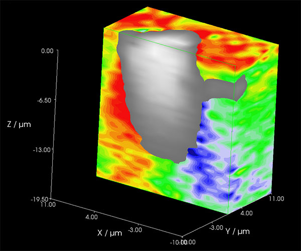
As a non-invasive and non-destructive technique, Raman is useful for characterising compound semiconductors. You can acquire sub-micrometre information about vibrational, crystal and electronic structure.
More details are available in an application note from Renishaw.
Analysing Silicon Carbide
Raman can be used to monitor and control the properties of silicon carbide raw materials and devices, to improve yield. These properties are greatly affected by:
- Crystal structure (SiC can exist in many polytypes)
- Crystal quality
- Defects (type and quantity)
All of these can be measured accurately with Raman spectroscopy. More details are available in an application note from Renishaw.
Quality Control
The Renishaw inVia Raman system can be implemented into production lines for online quality control analysis. This gives you the ability to detect problems quickly, thereby reducing waste and optimising yield.
With built-in automated calibration and health checks, you can rely on accurate, repeatable data.
More Information
If you have any questions or would like more information about Raman spectroscopy, please get in touch. Blue Scientific is the official distributor of Renishaw Raman in the Nordic region.
Contact us on +44 (0)1223 422 269 or info@blue-scientific.com
Renishaw inVia Raman Microscope