In-Situ Nanomechanical Testing Modes for SEM / TEM
Round-up of in-situ nanomechanical testing modes for electron microscopes (SEM and TEM). All of these modes can be added to your microscope with the Bruker Hysitron range of depth-sensing nanomechanical test instruments.
These systems interface with electron microscopes for quantitative nanomechanical testing together with simultaneous nanoscale imaging. As well as being able to position the probe extremely accurately, you can also view the deformation process throughout the test.
Blue Scientific is the official distributor for Bruker Hysitron instruments in the Nordic region (Norway, Sweden, Iceland, Finland, Denmark). For more information or quotes, please get in touch.
Bruker Hysitron instruments
More posts about electron microscopy
Contact us on +44 (0)1223 422 269 or info@blue-scientific.com
Testing Modes
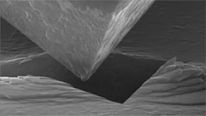
Nanoindentation
Measure mechanical properties including hardness and elastic modulus. Observe changes in material deformation at the nanoscale. A benefit of in-situ testing is the ability to position your test extremely accurately, to test specific points. Load and depth can also be controlled precisely at the nanoscale.
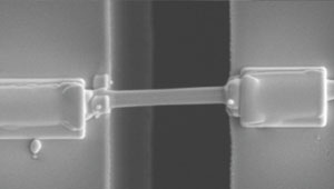
Tensile Testing
Measure stress-strain behaviour in low dimensional materials, which can be difficult to test using traditional methods. Accurate stress and strain values can be calculated directly from microscope measurements. Perform direct-pull and Push-to-Pull (PTP) testing on dog-bone specimens, thin films and nanowires. You can also observe dislocation initiation, pinning, interaction with defects and other deformation mechanisms, with quantitative direct pull tests.

Bend Testing
Analyse stiffness and fracture toughness easily. SEM imaging makes it simpler to measure size and align loading accurately. Suitable for single-phase, composite and layered materials.
In failure analysis you can observe, measure and analyse fractures at interfaces. You can also evaluate failure initiation points in multilayer devices by applying bending stresses to microbeams of layered, composite or multiphase structures.
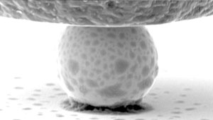
Compression
Compress pillars, particles and other small structures to measure stress-strain behaviour and yield strength. You can simultaneously observe deformation mechanisms in real time, for a full understanding of the material. Tip alignment can be verified by SEM/TEM imaging.
Particle compression test are useful for evaluating particles as potential components in engineered materials. Acquire data about size/strength relationships at the nano- and micro-scale.
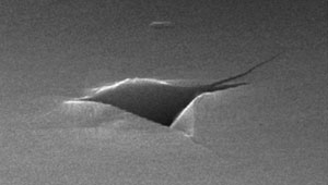
SEM and TEM Heating
Directly measure and observe material transformation caused by heating. Thermal testing is ideal for materials that need to be reliable under extreme conditions.
Two options are available for heating at temperatures up to 400°C and 800°C. You can then study deformation mechanisms such as brittle-to-ductile transitions in glass and polymers.
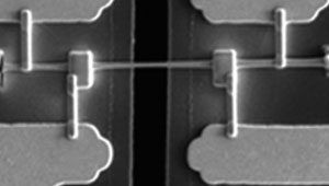
Electrical Characterisation
Simultaneously measure electrical and mechanical properties with an optional electrical characterisation module. These can be measured during nanoindentation, compression and tensile loading. This gives you an understanding of the roots of electrical property changes in various materials and devices.
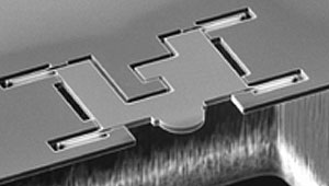
Push / Pull
Analyse the mechanical properties of 1D and 2D materials with an optional Push-to-Pull (PTP) device for SEM and TEM.
Mount a nano-tube or thin film and apply quantitative tensile loads. This enables you to calculate tensile properties, together with real-time videos from the electron microscope.
There’s also an electrical version (E-PTP: electrical Push-to-Pull) for four point electrical measurements during tensile experiments.
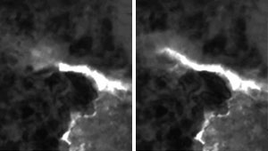
nanoDynamic Mode
NanoDynamic mode (optional upgrade) measures viscoelastic and fatigue properties as a function of depth and frequency, by applying an oscillating force.
This is ideal for biological materials, glass, polymers and certain types of metals, which have time dependent mechanical properties. This viscoelasticity make it difficult to completely describe the material response with traditional nanoindentation methods, but they can be measured continuously using nanoDynamic mode.
Instrumentation
These modes are available with Bruker Hysitron’s in-situ nanomechanical testing systems for TEM and SEM:
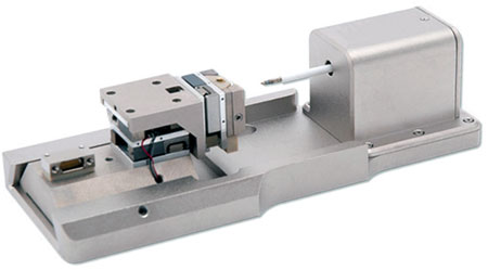
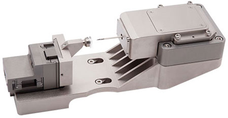
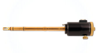
Hysitron PI 85L SEM PicoIndenter
Versatile, compact system
- Mounts directly to the SEM stage
- Maximum sample tilt and minimum working distance
- Low profile design for SEM, Raman / optical microscopes,
beamlines and more
Hysitron PI 88 SEM PicoIndenter
Most comprehensive platform
- Truly quantitative nanoscale mechanical characterisation with direct observation
- Optional tilt and rotation stage for advanced XYZ sample positioning
- Modular design for the full suite of techniques
More info…
Hysitron PI 95 TEM PicoIndenter
For TEM
- First full-fledged depth sensing indenter for TEM
- Testing modes include indentation, compression, tensile, bend and scratch
- Compatible with all major TEM models
[hr]
Further Information
Blue Scientific is the official Nordic distributor for Bruker Nano Surface Analysis instruments, including the Hysitron range. If you’d like any further information, quotes or demonstrations, please get in touch:
Contact us on +44 (0)1223 422 269 or info@blue-scientific.com
Bruker Hysitron instruments
More posts about electron microscopy


