Analysing Ultra-Wide Bandgap (UWBG) Semiconductors with Cathodoluminescence (CL)
Ultra-wide bandgap (UWBG) semiconductors offer significant benefits in electronic and optoelectronic technologies. High-quality, low defect materials are required for commercial device development. However, conventional semiconductor process development methods such as photoluminescence spectroscopy can’t be used on UWBG.
SEM-based cathodoluminescence can be used to map UWBG semiconductor materials at the nanoscale, to map defects and variations and ensure high quality materials in process development.
Blue Scientific is the official distributor for Gatan systems for electron microscopes in Norway, Sweden, Denmark, Finland and Iceland. For more information or quotes, please get in touch.
Gatan Monarc
Articles about cathodoluminescence
Contact us on +44 (0)1223 422 269 or info@blue-scientific.com
Ultra-Wide-Bandgap Semiconductors
Ultra-wide bandgap (UWBG) materials such as Al(Ga)N, Ga2O3, BN and diamond have notable benefits for high power and high frequency electronic and optoelectronic devices operating at deep UV wavelengths. They’re also useful in environments where radiation damage or high temperatures are a factor, where other materials may not be suitable.
An Alternative to Photoluminescence
For commercially viable devices, it’s important that the materials used are high quality, without defects. However, conventional photoluminescence methods can’t be applied, because UWBG materials are transparent at the wavelengths commonly used in process development.
Cathodoluminescence (CL) is an alternative spectroscopic technique that’s suitable for UWBG semiconductors. It can be used to map defects and examine variations in materials at the nanoscale – ideal in the development of materials for semiconductor devices.
What is Cathodoluminescence?
Cathodoluminescence is an analytical technique for characterising composition, optical and electronic properties. The results correlate with morphology, micro-structure, composition and chemistry at the micro- and nanoscale.
CL can easily be added to your electron micoscope (SEM, TEM or STEM) with systems from Gatan.
More about cathodoluminescence and how it’s used
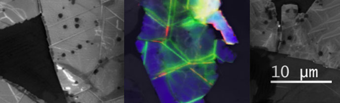
Example: Hexagonal Boron Nitride (h-BN)
In this example, spectroscopic cathodoluminescence was used to analyse hexagonal boron nitride (h-BN) with a bandgap of ~5.5 – 6.0 eV.
In an SEM (Scanning Electron Microscope) a focused electron beam was used to excite electron-hole pairs in the h-BN. A Gatan Monarc Pro cathodoluminescence system was employed to captured and analysed the radiative decay of excess carrier results in the emission of photons.
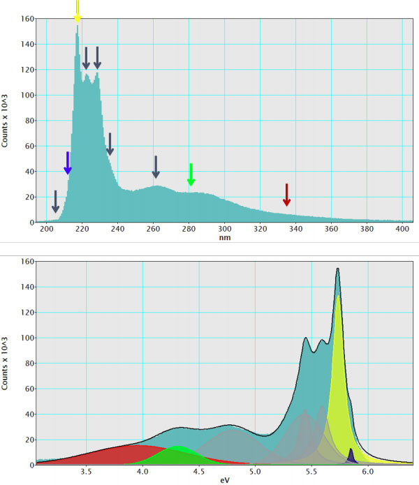
Hyperspectral data was collected via spectrum imaging, collecting both spatial and spectral information. This involves scanning the SEM beam across the specimen surface and acquiring a wavelength-resolved spectrum at each location.
Near-bandgap luminescence (200 – 400 nm, 3.10 – 6.19 eV) associated with Frenkel excitons and defect / impurity colour centres was analysed at room temperature. Deconvolution of the spectrum using non-linear least squares (NLLS) fitting revealed nine peaks corresponding to near-bandgap exciton emission and mid-gap colour centers. The black line is the sum of all models, demonstrating an excellent fit to the raw data.
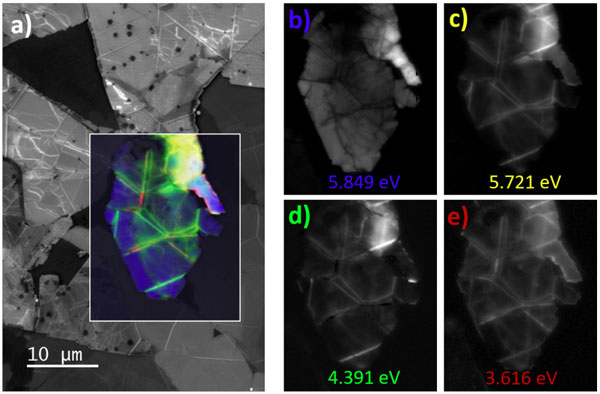
Strong spatial variation is apparent between emission lines, shown on maps extracted by non-linear least-squares fitting. The colourised image below in a) is a composite of maps b) – e). The colour coding on the maps corresponds with the spectra above.
This demonstrates how cathodoluminscence can be used to analyse UWBG semiconductors at room temperature.
Full details of the measurement are available in an experiment brief from Gatan.
Instrumentation: Gatan Monarc
SEM-based cathodoluminescence system:
- Sharp spectra and images.
- Map defect distribution and variations in exciton behaviour.
- High spatial resolution.
- Large field of view.
- Fast data collection.
- Users of all experience levels can capture high quality data.
More Information
Blue Scientific is the official distributor of Gatan systems for electron microscopes in the Nordic region. We’re available to answer all your questions – just get in touch: