What is Cathodoluminescence? Plus how to add it to your SEM/TEM/STEM
Cathodoluminescence (CL) is a scientific analytical technique for characterising composition, optical and electronic properties. This data correlates with morphology, micro-structure, composition and chemistry at the micro- and nanoscale.
This technique can easily be added to your electron micoscope (SEM, TEM or STEM) with systems from Gatan.
Blue Scientific is the official Nordic distributor for Gatan systems for electron microscopes in Norway, Sweden, Denmark, Finland and Iceland. For more information or quotes, please get in touch.
View the Gatan range
Contact us on +44 (0)1223 422 269 or info@blue-scientific.com
Follow @blue_scientificWhat is Cathodoluminescence?
Cathodoluminescence (also known as CL) is the emission of photons as light, when a material is stimulated by high energy electrons.
Cathodoluminescence microscopy involves analysing the light or photons (luminescence) that are emitted when a sample is stimulated by the electron beam of an electron microscope. This beam can be focused at sub-nanometer length scales, so you can go beyond going beyond the diffraction limit constraints of optical microscopes, and study optical properties at the nanoscale.
Cathodoluminescence data can also be correlated with other signals, to reveal more information about your sample.
What can you Analyse?
CL can be used in a SEM or STEM (Scanning or Scanning Transmission Electron Microscope) to characterise materials:
- Composition
- Optical properties
- Electronic properties
This data correlates with morphology, micro-structure, composition and chemistry at the micro- and nano-scale.
Advantages of Cathodoluminescence
While there are other techniques for measuring optical properties (eg optical emission spectroscopy, photo-luminescence, electro-luminescence) SEM-based CL has several unique advantages:
- Sub-nm spatial resolution
- Data correlates with structural information
- Wealth of data from the emitted signals: morphology (eg size and shape), composition, chemistry, crystallography, electronic properties and more
Unique Benefits
These advantages can be used to perform unique studies:
- Study the optical properties of individual nanostructures and assemblies with optical characterisation below the diffraction limit.
- Analyse semiconductors: Growth, composition and quantify point and extended defect distributions
- Characterise optical materials and devices with a spatial resolution better than the diffraction limit of light
- Reveal texture in minerals – Reconstruct geochemical processes by revealing trace element distributions
- Measure morphology and composition simultaneously – Fully characterise your sample, correlating shape, size, crystallinity and composition with optical properties
- Analyse properties without manufacturing a complete device and take non-destructive measurements
Application Areas
The ability to measure optical properties at such a small scale is useful in many areas, including:
- Light emitting diodes (LEDs)
- Nanoparticles
- Oil and geology
- Optoelectronic and photovoltaic materials
- Solar cells
- Phosphors
- 2D materials
- Pharmaceuticals
- Polymers
- Plasmonics (noble metals)
- Organic materials
To find out whether CL could be used in your area of research, please get in touch.
Electronics and Optoelectronics
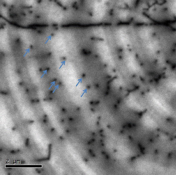
Measure the local electronic band gap in semiconductors and study defect distribution at the micro- and nano-scale. This enables you to examine direct bandgap semiconductors with strong cathodoluminescence (eg GaAs or GaN), as well as indirect semiconductors that emit weak cathodoluminescence (eg silicon).
Variations in luminescence caused by perfect and dislocated crystalline silicon can be used to map defects in integrated circuits. The high spatial resolution is ideal for low-dimensional semiconductor structures such as quantum wells and dots.
Example: Mapping defects on UWBG semiconductors
Geoscience
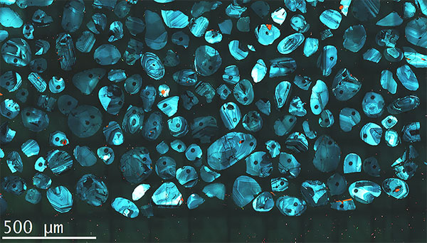
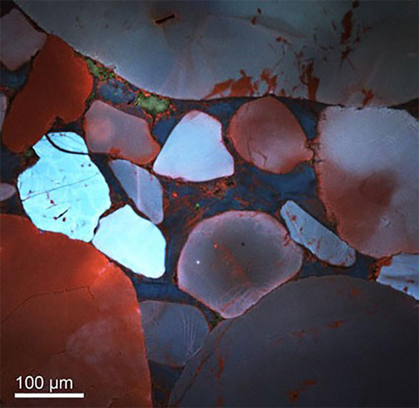
Studying trace element chemistry and geochemical effects enables you to reconstruct geological processes in rocks and minerals. SEM-based cathodoluminescence reveals internal structures not visible using other techniques. This gives you access to unique information about mineral composition, growth and provenance.
More about SEM-based CL in geology and geoscience
Material Science
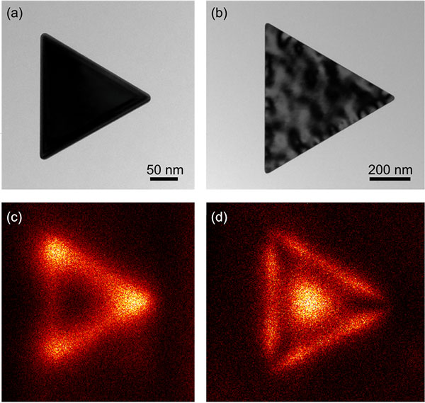
Cathodoluminescence is useful in the development of sensor and communication technologies that involve the interaction of light with metal nanoparticles. Their properties can be measured by surface plasmons and local surface plasmon resonance modes.
There have also been recent publications involving the use of SEM-based cathodoluminescence for studying surface plasmon resonance in metallic nanoparticles, with resolution below the diffraction limit.
Organic Molecules and Pharmaceuticals
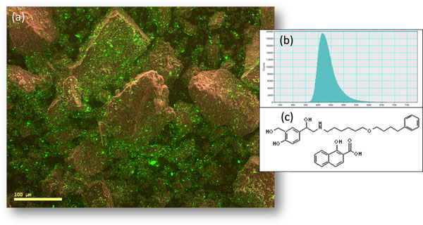
Many polymers and active ingredients in pharmaceuticals are cathodoluminescent. The signal reveals the chemical structure of molecules, so it can be used to map the distribution of organic molecules with sub-100 nm resolution.
Instrumentation
These systems can be used to add cathodoluminesence to your SEM/TEM. They’re compatible with electron microscopes from major manufacturers – contact us for details.
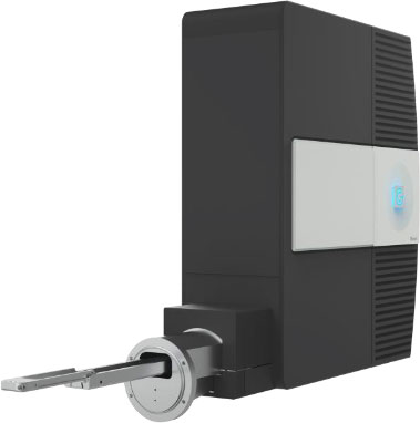
Monarc CL Detector
Next generation system for SEM
- Unmatched spatial, angular and wavelength resolution
- Collect hyper-spectral data 30x faster than other CL detectors
- Large field of view
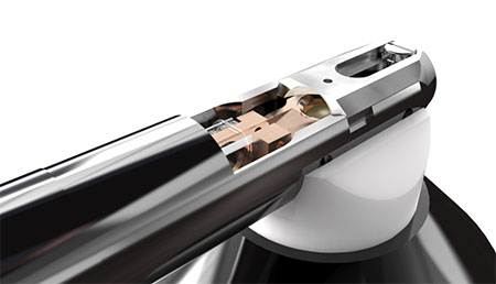
Vulcan CL Detector
For TEM/STEM
- Analyse a wide range of samples
- Combine with other techniques
- Compatible with Gatan EELS systems for correlating absorption and emission processes
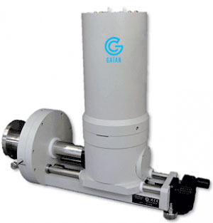
ChromaCL2 iBSED Detector
For geology and geoscience
- Live, colour CL imaging
- Reveal geochemical processes
- Visualise texture easily
- Automated montages for a large field of view
More Information
Blue Scientific is the official distributor of Gatan systems for electron microscopes – including their state-of-the-art cameras, filters and sample preparation equipment. We’re here to provide quotes and help with any queries you have about how they can enhance the capabilities of your microscope – just get in touch:


