+44 (0)1223 422 269 Contact

Category Archive for ‘Nano Surfaces’

Semiconductor wafer

Characterising CMP Pads with Nanoindentation

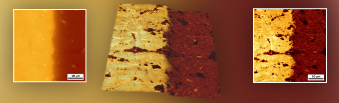
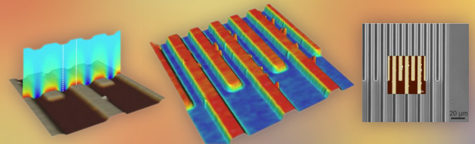
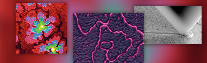
How to use dynamic nanoindentation characterise CMP pads. In this example, the Bruker Hysitron TS 77 Select was employed to quantitatively measure the viscoelastic properties of a hard pad.

This is a robust, reliable method for examining CMP pad surface quality and processes.

Scientific Nanoscale Analysis Podcast

“Solutions for NanoAnalysis” Podcast

A new nanoanalysis podcast from Bruker, with special guests from all areas of nanoscale analysis including micro-XRF, TXRF, nanomechanical testing, TEM/SEM and more.

Bruker AFM Contact Resonance Module

New Bruker BioAFM Contact Resonance Module for Stiff Biological Samples

Bruker’s Contact Resonance module is for mechanical characterisation of stiff biological samples, polymers and metals with AFM (Atomic Force Microscopy). Until now it was not possible to study the nanomechanical properties of samples such as teeth, bones, seeds, wood and medical implants with this level of accuracy.

Bruker Ringing Mode AFM

Bruker Ringing Mode for Surface Adhesion Property Mapping with AFM

Ringing Mode is a new Bruker AFM mode for enhanced surface adhesion property mapping.

Bruker JPK BioAFM SECM

New SECM (Scanning Electrochemical Microscopy) Option for Bruker JPK BioAFM

A new Scanning Electrochemistry option is available for the Bruker JPK NanoWizard BioAFM series. AFM-based SECM is used for electrochemical mapping at nanoscale resolution.

AFM in Virus Research

AFM in Virus Research

How Atomic Force Microscopy can be used in virology, including measuring biomechanical properties and virus-cell receptor interactions.

In-Situ Material Deformation Testing

In-Situ Nanomechanical Test System for Analysing Material Deformation in SEM

The new Bruker Hysitron PI 89 SEM PicoIndenter is an in-situ nanomechanical testing system for electron microscopes, for analysing deformation of high-strength materials.

Bruker ContourX 3D Optical Profilers

New Bruker ContourX 3D Optical Profilers

A new range of Bruker ContourX benchtop 3D optical profilers for roughness metrology, surface texture metrology and fully automated 3D metrology. Blue Scientific is the official distributor for Bruker Nano Surface Analysis instruments in Norway, Sweden, Denmark, Finland and Iceland. For more information or quotes, please get in touch. Bruker Nano Surface Analysis range  Contact us on […]

GaN Nanowire Defects

Studying Defect Formation in GaN Structures with AFM

Lund University in Sweden recently published two scientific papers about studying defects in GaN nanowires and structures, using AFM and various complementary techniques.

Online Training from Bruker Nano

Online Training from Bruker Nano: AFM, Tribology, Nanoindentation and more

Join Bruker for a series of free online training sessions over the next few weeks, covering nanoscale surface analysis topic.