Identifying Contaminants on Semiconductors with Nanoscale IR Spectroscopy
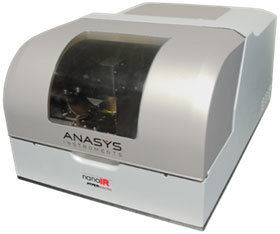
The Bruker Anasys nanoIR3 is a complete nanoscale FTIR, chemical imaging and characterisation platform, ideal for failure analysis and materials characterisation.
Unambiguously identify organic nano-contaminants on wafers, media and slider substrates. In addition to this you can also acquire mechanical, thermal and structural property information with nanoscale spatial resolution.
Bruker Anasys nanoIR3
Application Note: Characterising Semiconductor Films
Contact us on +44 (0)1223 422 269 or info@blue-scientific.com
Identify Organic Nano-Contaminants
Organic nano-contaminants are a well-known cause of defects in micro-electronics manufacturing, including semiconductors, data storage devices and LEDs. They can cause yield issues, manufacturing delays and even scrap products.
Contamination can come from many sources, including chemical processing, cleaning, airborne molecular contamination, wafer transfer / handling and manual interaction. Accurate identification is key to tackling the problem. However, particularly in the case of organic nano-contaminants, identification is often ambiguous because of insufficient resolution and even sample damage during analysis.
With AFM-IR you can identify contaminants unambiguously, with precise, reliable data and standard FT-IR databases. In addition to this, you also can also analyse multiple properties with nanoscale resolution.

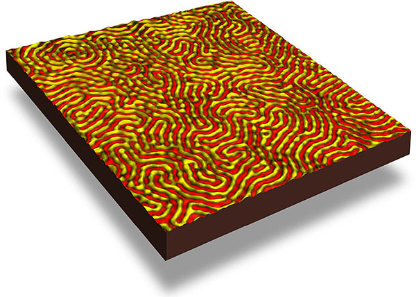
Block co-polymer surface analysed with AFM-IR at 10nm chemical spatial resolution.
Patented AFM-IR Technique
AFM-IR goes beyond the limitations of other characterisation methods when analysing organic nano-contaminants and semiconductor defects. It’s a breakthrough analytical technique involving infrared spectra at spatial resolutions down to 10 nm, giving you access to nanoscale chemical fingerprints. AFM-IR is a patented technique, available using the Bruker Anasys nanoIR3 nanoscale IR spectrometer.
The spectra acquired from AFM-IR correlate directly with traditional FTIR spectra, so you can use standard FTIR libraries. As well as chemical analysis data, you also have access to mechanical, electrical, thermal and structural property information – all at nanoscale spatial resolution.
nanoIR3
The nanoIR3 is a nanoscale FTIR, chemical imaging and materials characterisation platform ideal for studying:
- Nano-organic contaminants
- LowK dielectrics
- Semiconductor materials
- Data storage media and slide
Example: Nano-Contamination on a Silicon Wafer
In this example, contaminated silicon wafers were prepared using materials from semiconductor manufacturing environments. Tapping AFM-IR imaging was then used to locate the contamination, followed by AFM-IR for identification.
The AFM height image below shows the thickness variation (20-100nm) of the contaminant residue on the wafer. AFM-IR spectra were then acquired from points with variable thickness. As you would expect, the IR intensities vary with the sample thickness. However, the overall signal to noise ratio is sufficient to identify the material accurately as human skin tissue. The sensitivity of AFM-IR makes it possible to analyse thin samples; here the contamination could be identified even at 20nm thickness.
![]()
Example: PET Contamination
Unique FASTspectra technology rapidly acquires spectra over the full IR tuning range. This reduces acquisition time by a factor of 10, while still maintaining a high level of accuracy.
In the example below, ~30 nm tall contamination residue was measured with the nanoIR3. The AFM-IR spectra below were matched to commonly used FTIR database (KnowItAll from Bio-Rad Inc.). The residue was identified as polyethylene terephthalate (PET), which is typically used in polyester fabrics. FASTspectra data was used for this identification, demonstrating the high level of accuracy even with the fast acquisition.
PET contamination on a silicon wafer: (a) AFM height image; (b) FASTspectra data on (red) and off (blue) the contaminated area; (c) The contaminant is positively identified as PET, using an FTIR database.
Instrumentation
The Bruker Anasys nanoIR3 is a nanoscale IR spectrometer, ideal for identifying nanoscale organic contaminants in semiconductor fabrication, and in other electronic devices.

- True model-free nanoscale IR absorption spectroscopy
- Correlative microscopy with nanoscale property mapping and full featured AFM
- Sub-10nm chemical imaging resolution with Tapping AFM-IR
- Nanoscale material property mapping
- High resolution spectroscopy in seconds
- Direct correlation with standard FTIR databases
Further Information
Blue Scientific is the official Nordic distributor of Bruker Anasys instruments. For more information, demonstrations or quotes please get in touch.
Information about this application is also available in an application note from Bruker Anasys.
Contact us on +44 (0)1223 422 269 or info@blue-scientific.com
Bruker Anasys nanoIR3
Banner image: Wikimedia Commons (Peellden)

