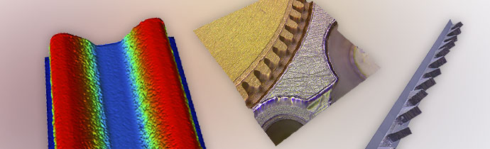
Achieve the highest lateral and vertical resolution with AcuityXR technology on Bruker’s Contour 3D optical microscopes. Break the optical diffraction limit, without compromising the other benefits of white light interferometry. For a limited time, we currently have a trade-in offer to help you benefit from the latest 3D optical microscope technology. Trade in your surface […]

How nanoscale infrared spectroscopy can be used to measure semiconductor materials in defect and contamination analysis, and fabrication.
How to analyse layers and coatings with Raman spectroscopy, with the example of paint on coated metal.
Cathodoluminescence (CL) is a technique for characterising composition, optical and electronic properties with data that correlates with morphology, micro-structure, composition and chemistry at the nanoscale.
New Bruker Contour LS-K 3D optical profiler for fast, high quality surface maps and metrology data, with new technology for focus variation on samples with topography.
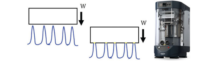
The amount of sliding friction between two surfaces is affected by a number of factors, one of the most obvious being surface texture. But how exactly does the roughness or smoothness of a surface affect its sliding friction? And what about different situations, such as elastic deformation? Donald K. Cohen PhD has published an interesting article […]

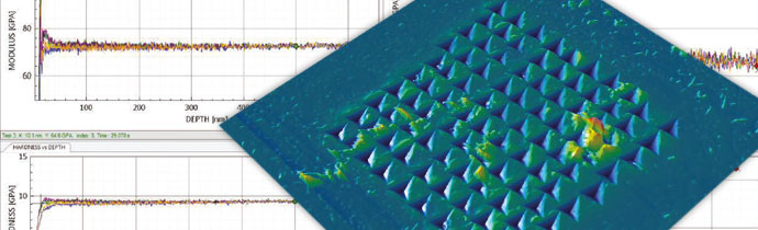
New nano-scratch option for the Bruker NanoForce nanomechanical testing system, for nanoscale scratch testing.